
MIKU
Introduction
I chose the MIKU Baby Monitor to be my spare-time exercise project. The reason being is that first of all: I already had the outer CAD surface (STP), which I used back in 2017 for a project as a freelance artist; and second of all the ability to show the internal PCB stuff and electronics I wanted to try to work with as a CG artist.
Besides working with PCBs, this object is a render-challenge for several more reasons. First, there is the need to render the "white-on-white", which is a good practice for classic high-key lighting.
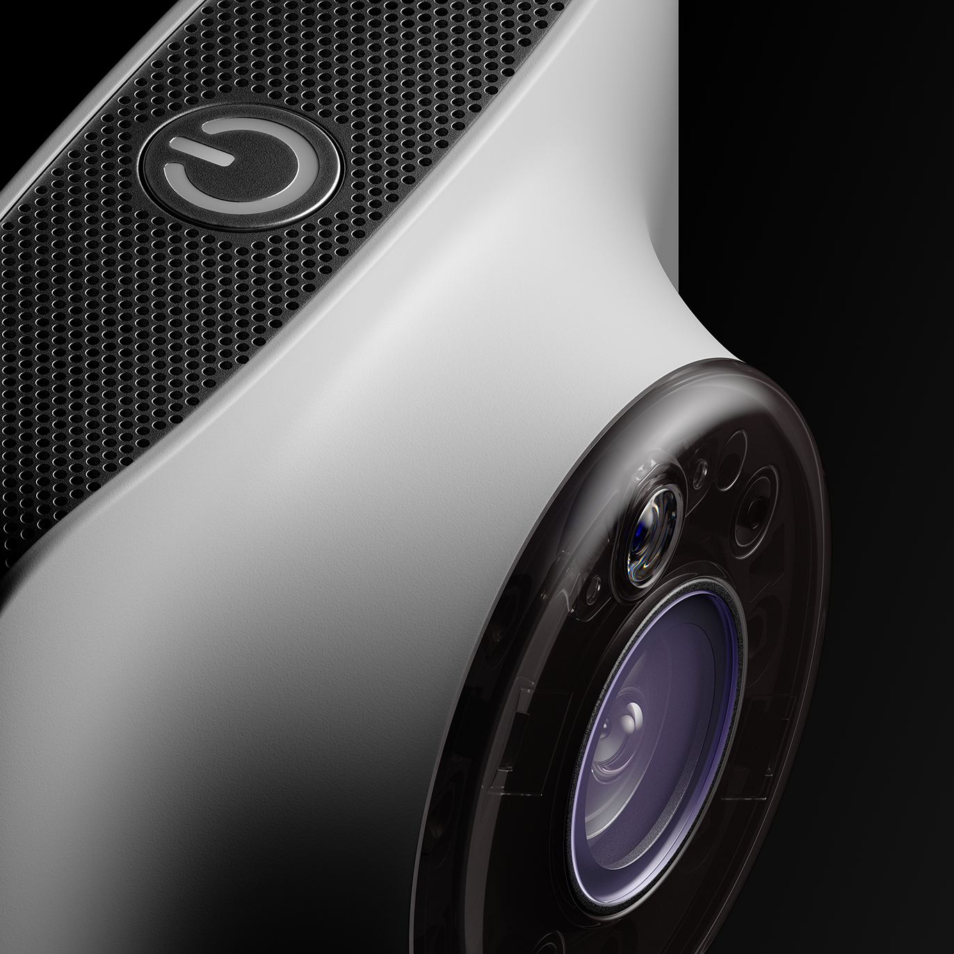
The second is that the object has an open camera lens, and I think that the look of the camera lens is the key moment in such projects. While the case lighting can be done in many different ways and looks good, camera lens lighting has a much more limited number of options how it can be well shown. Thus, in choosing the lighting style for MIKU, I was limited by how good the lens looked with the chosen lighting scheme, which created additional professional excitement.
I used the 3dsmax and the GPU rendering engine FStorm on this project. The project consists of five parts:
1. Renders of exterior case surface on a white background
2. Renders of internal electronics and open case
3. Transparent case with visible PCB inside and the explosions
4. Renders on a dark background.
2. Renders of internal electronics and open case
3. Transparent case with visible PCB inside and the explosions
4. Renders on a dark background.
5. Making off and behind the scenes.
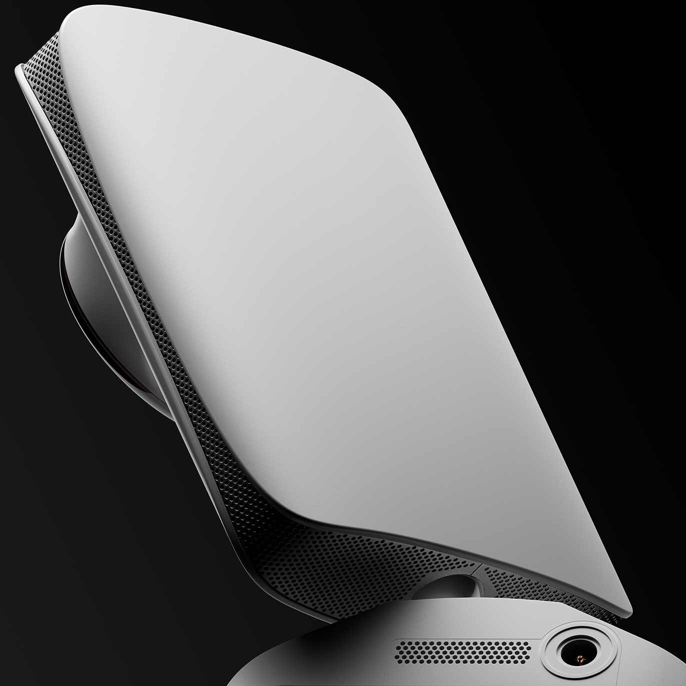
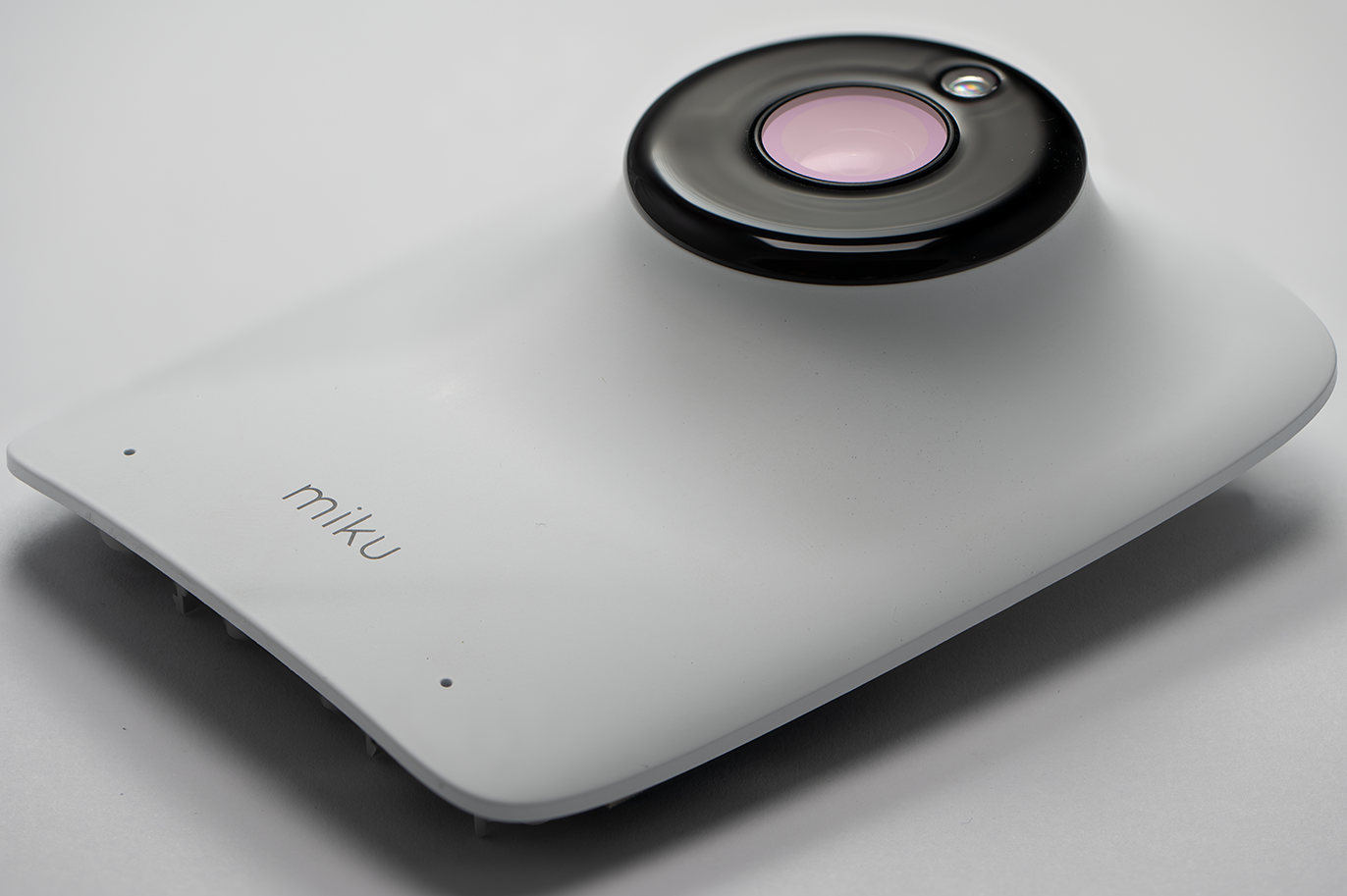
Renders on a white background
For this part of the project, I have chosen a look that can be called “formal”. There are no wide angles here, and I wanted to show the object as neutral and restrained as possible.
As I mentioned before, rendering a pure-white object on a white background itself is a pretty exciting challenge for me as a lighting artist.

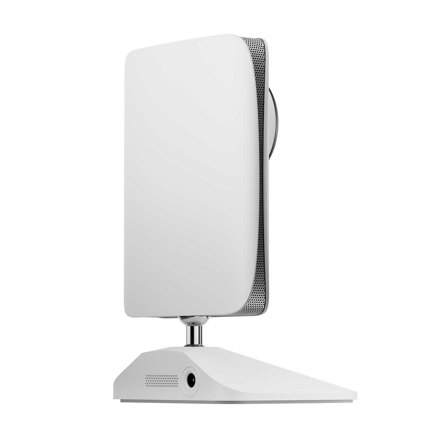
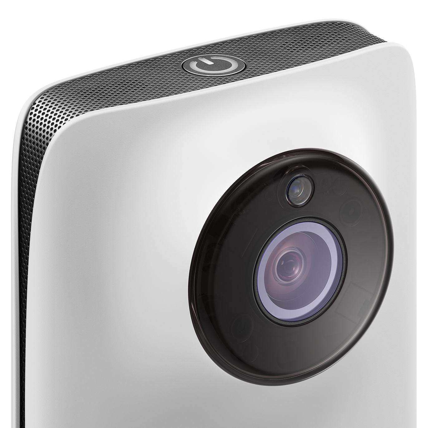
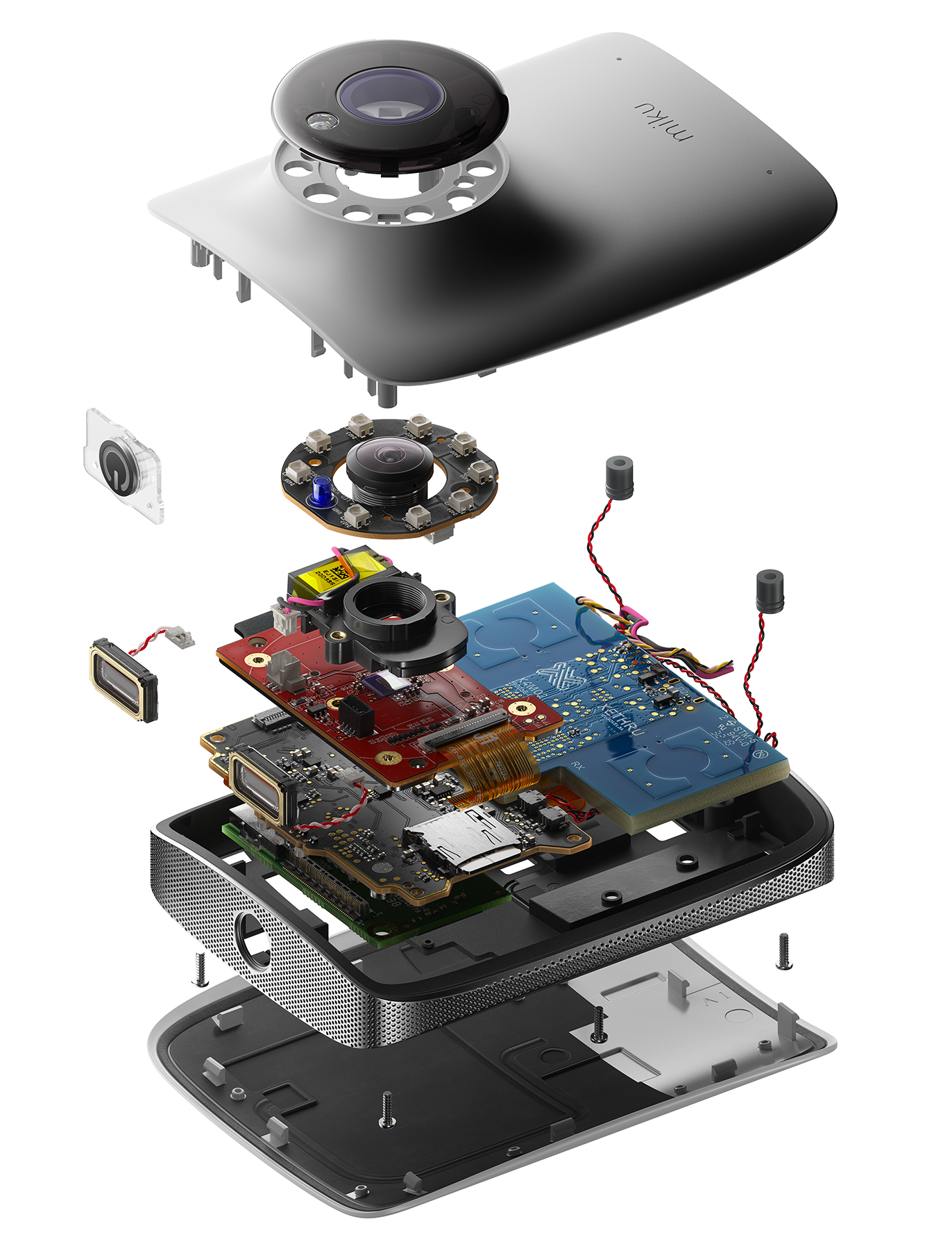
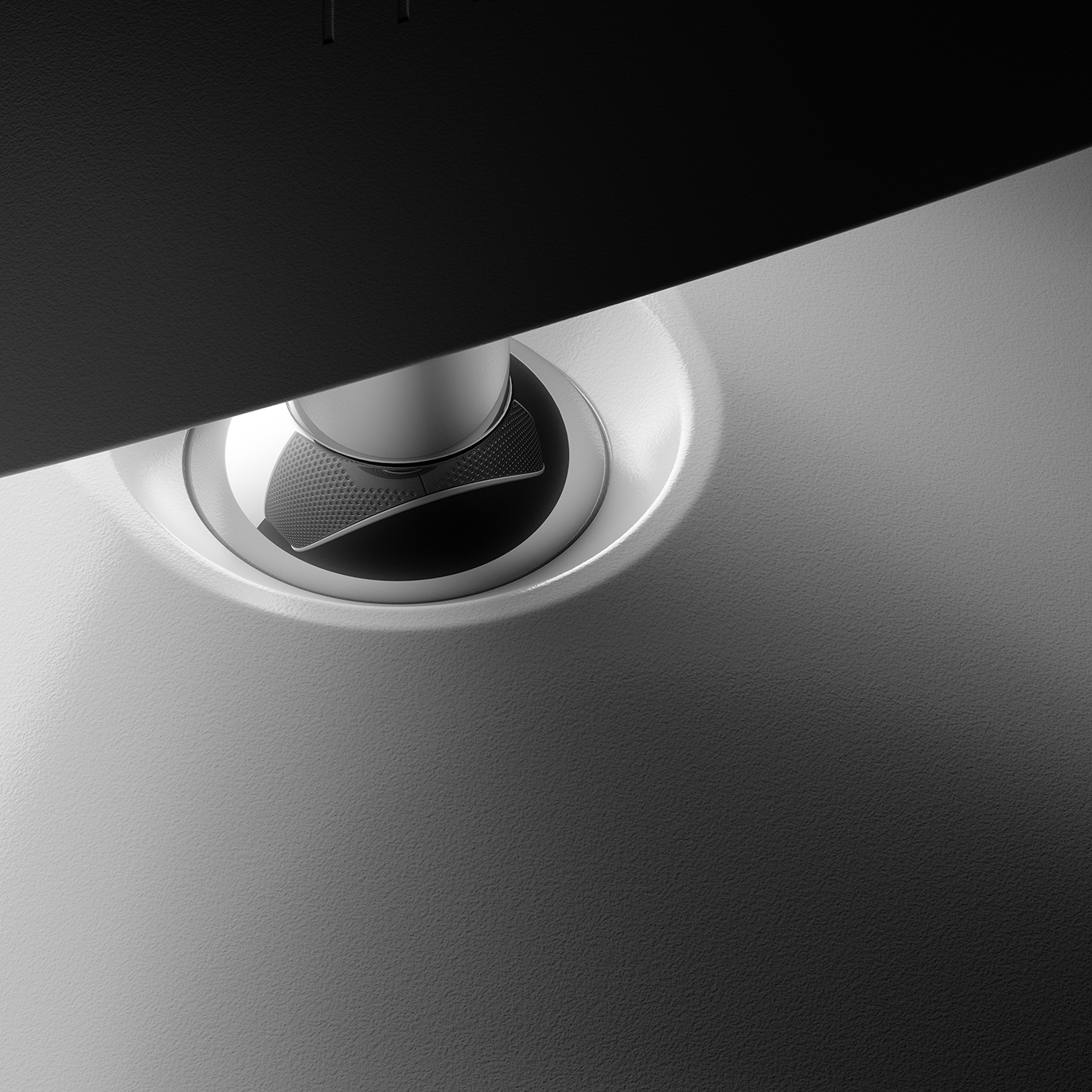
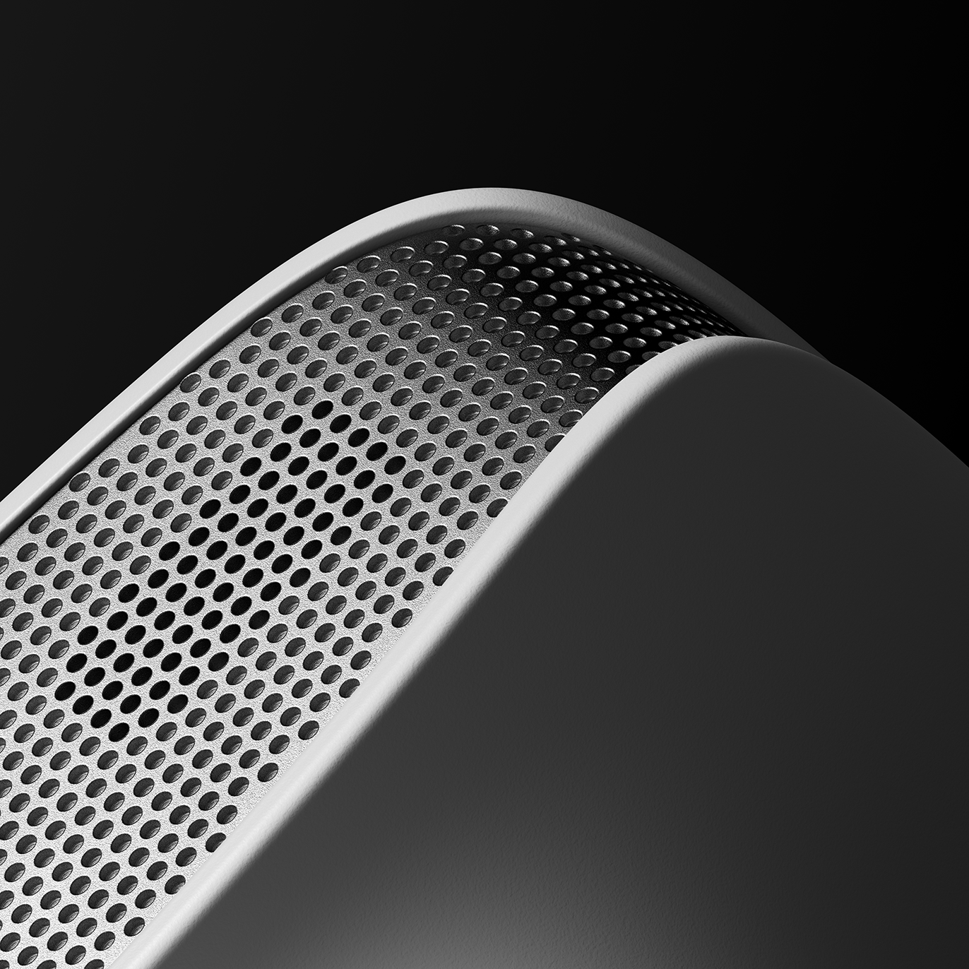
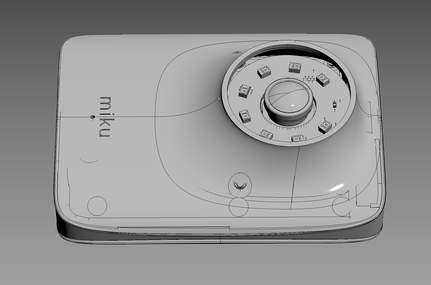
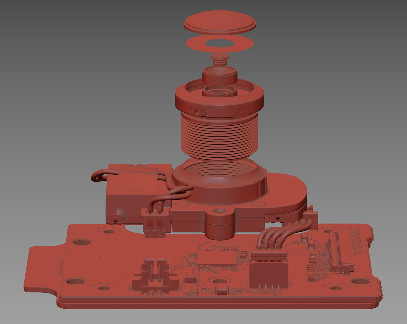
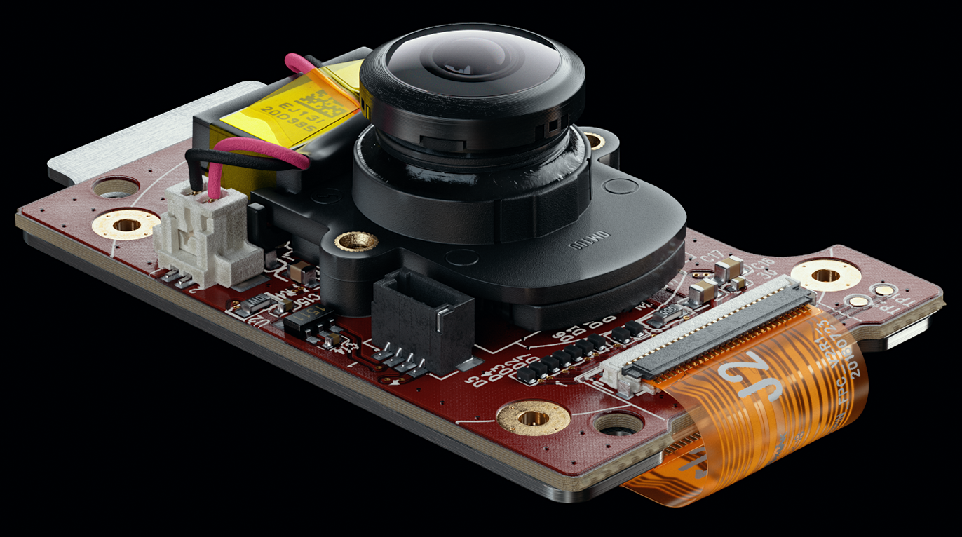
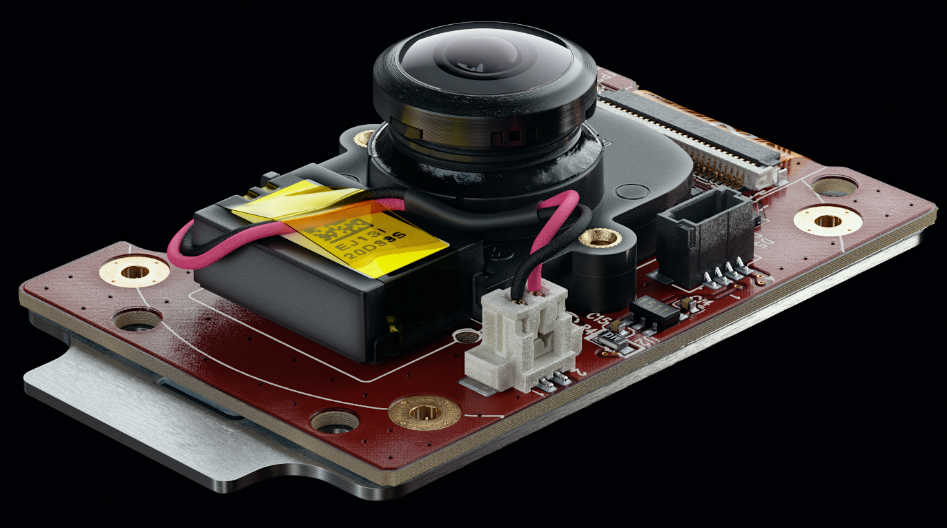
The main texture of the MIKU body is dull white plastic. On the front panel of the case, there is a lens cover cap which is black and glossy made of semi-transparent plastic. Besides the camera lens, there is also a group of IR illumination elements under it.

Open 4K Image
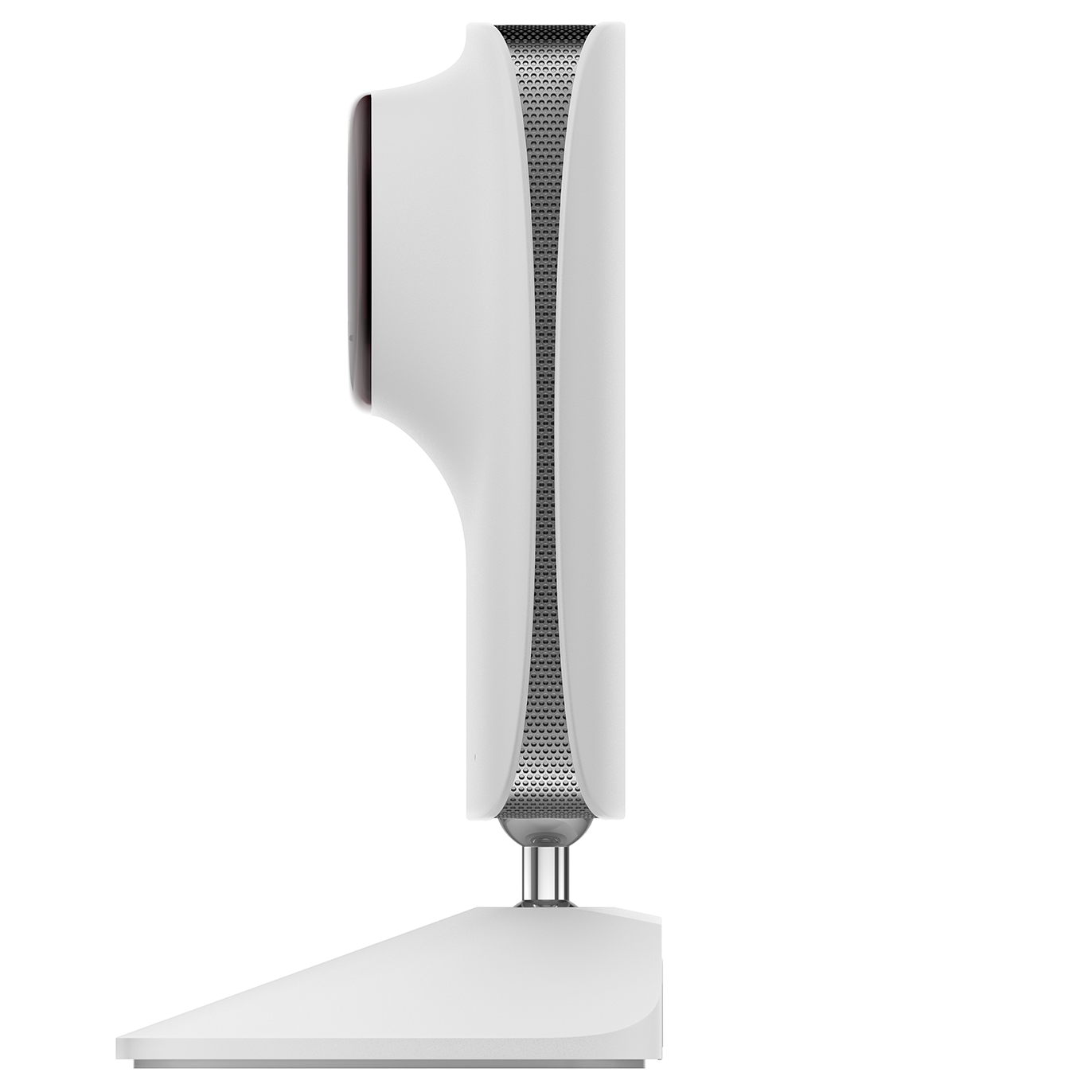


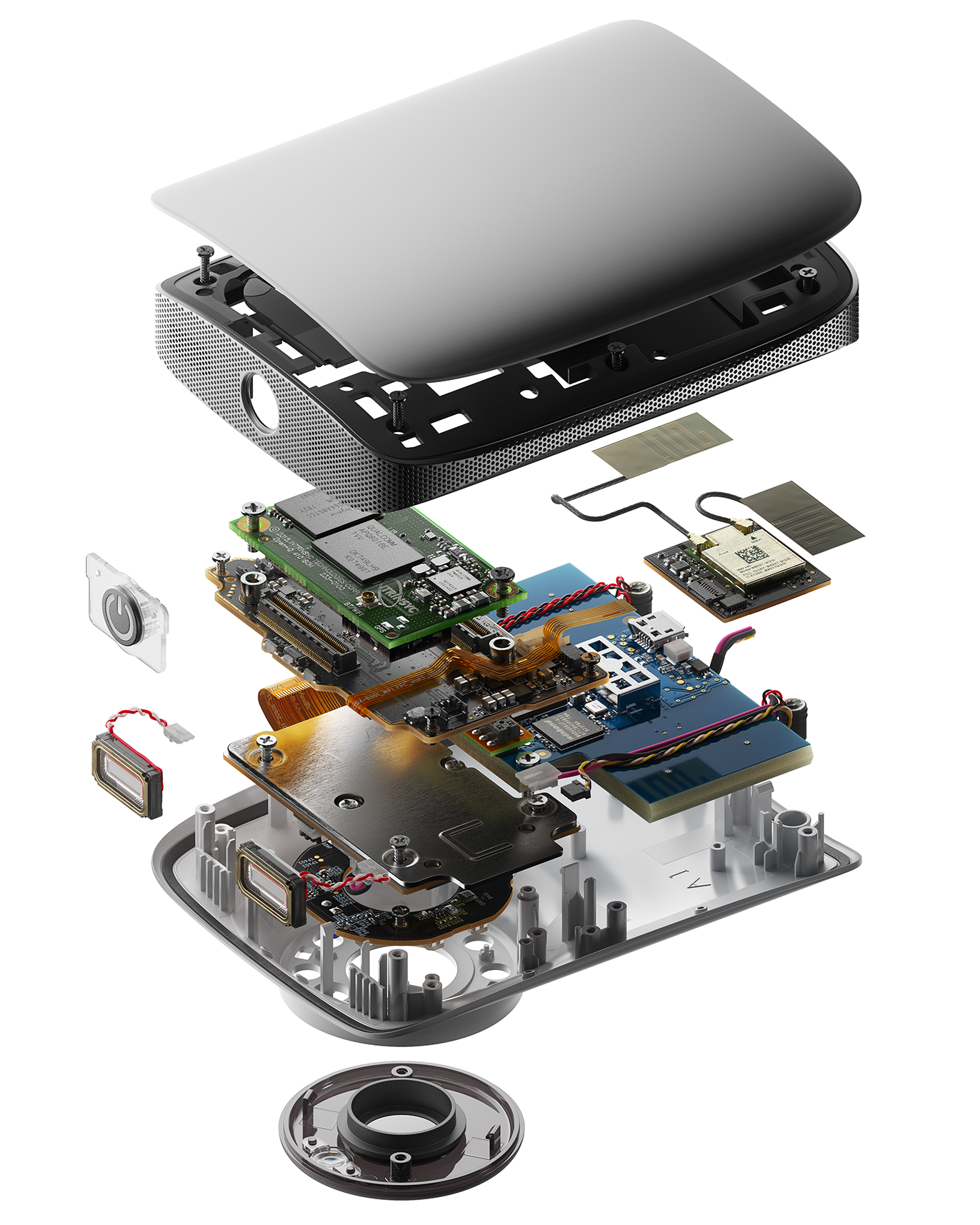
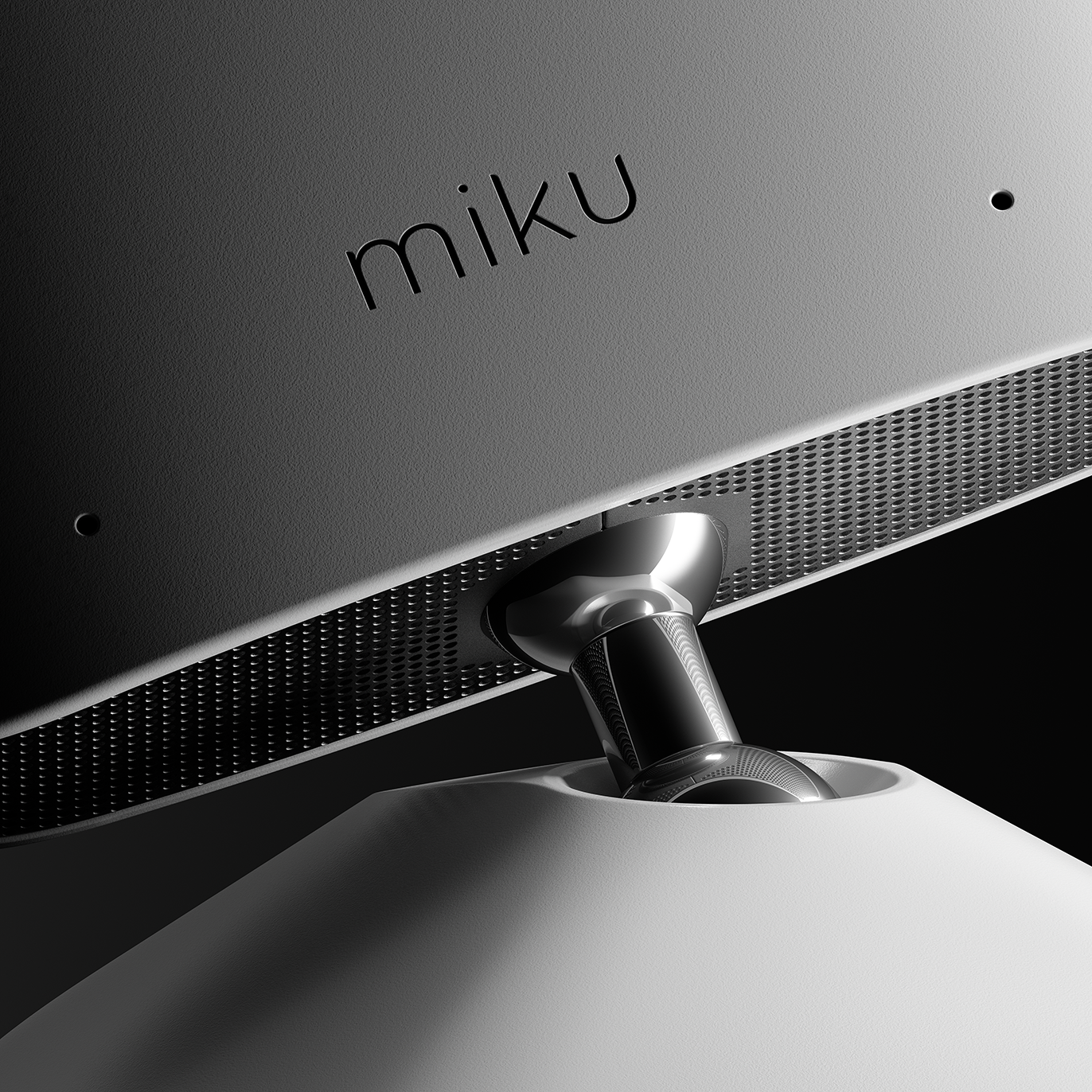
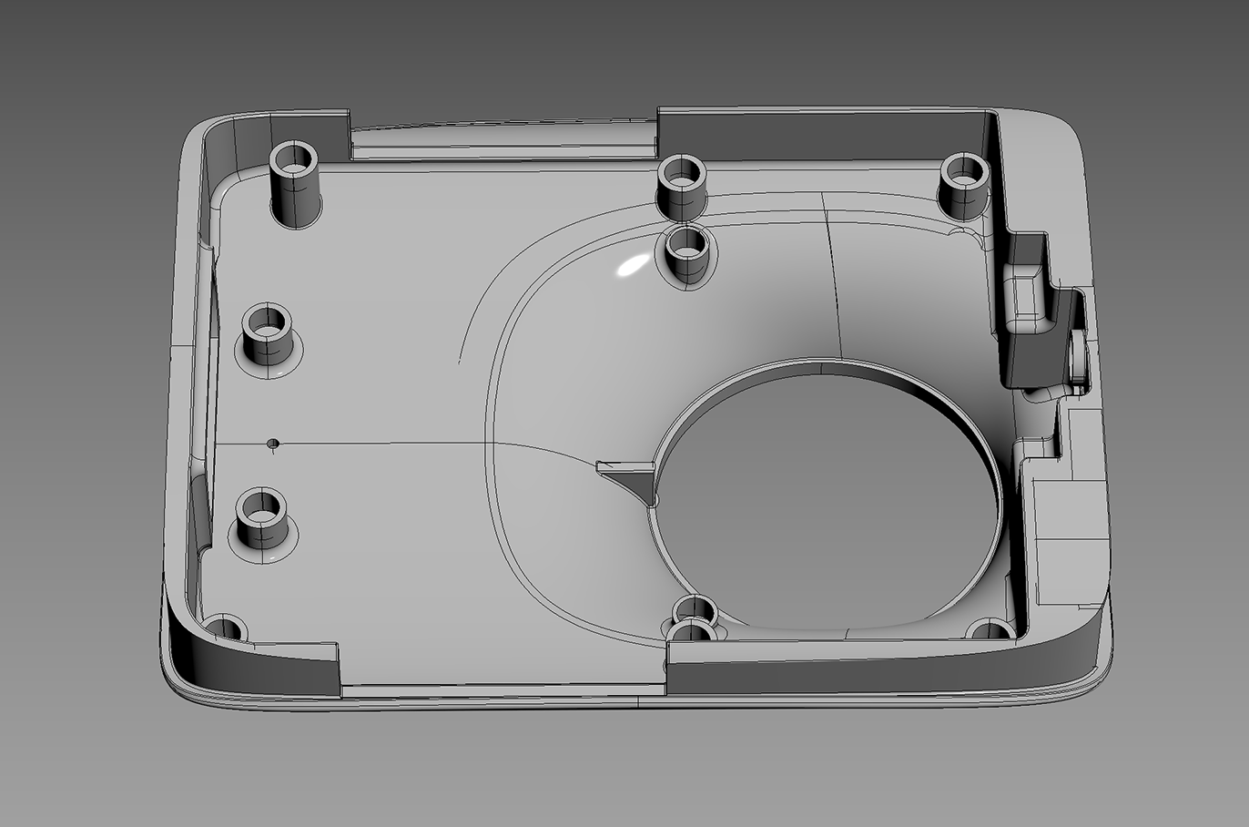
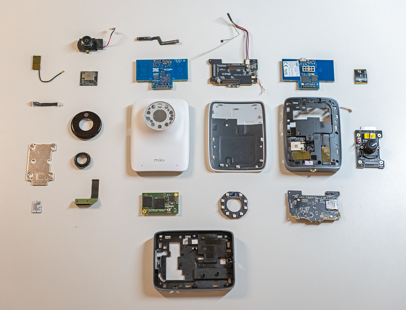
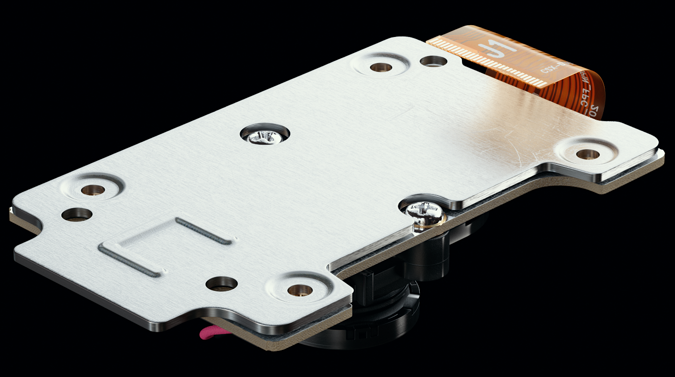
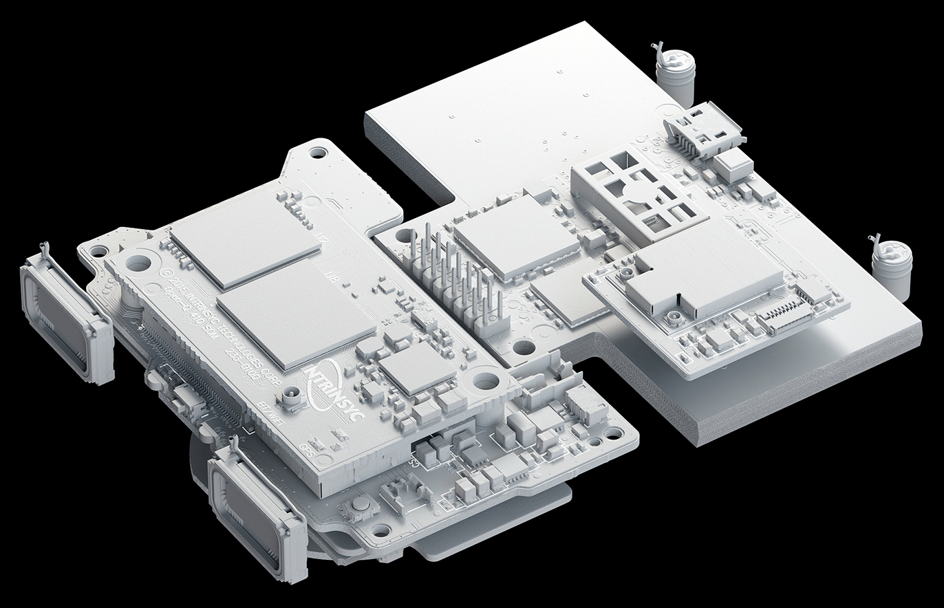
The baby monitor itself consists of a case and a mounting shoe with the power control electronics inside. A hinge connects these two parts so the body with the camera can orient in any direction. The side panel of the case originally was made of anodized aluminum, later was replaced with metalized plastic to reduce the production cost.

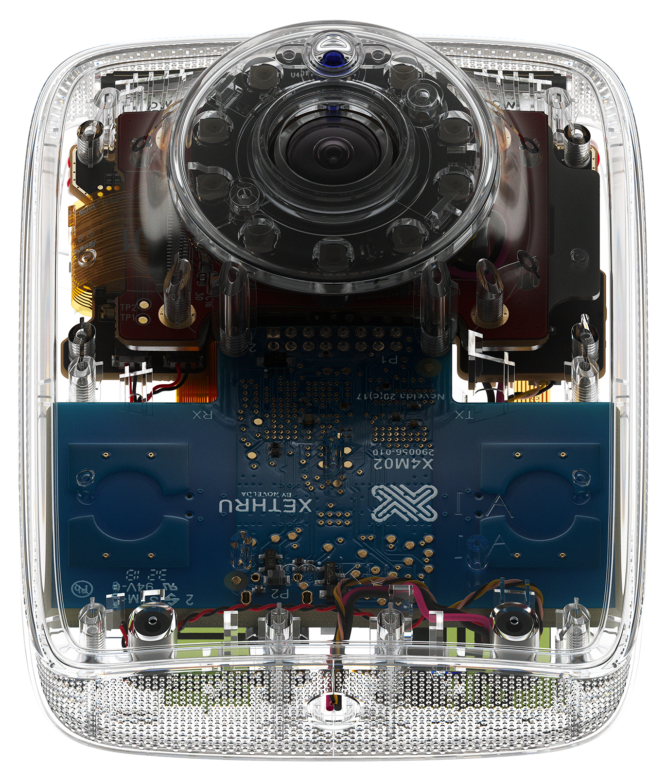
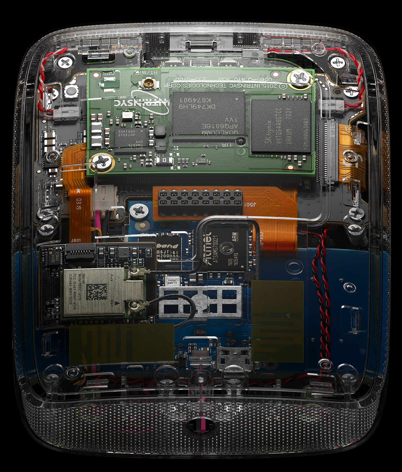
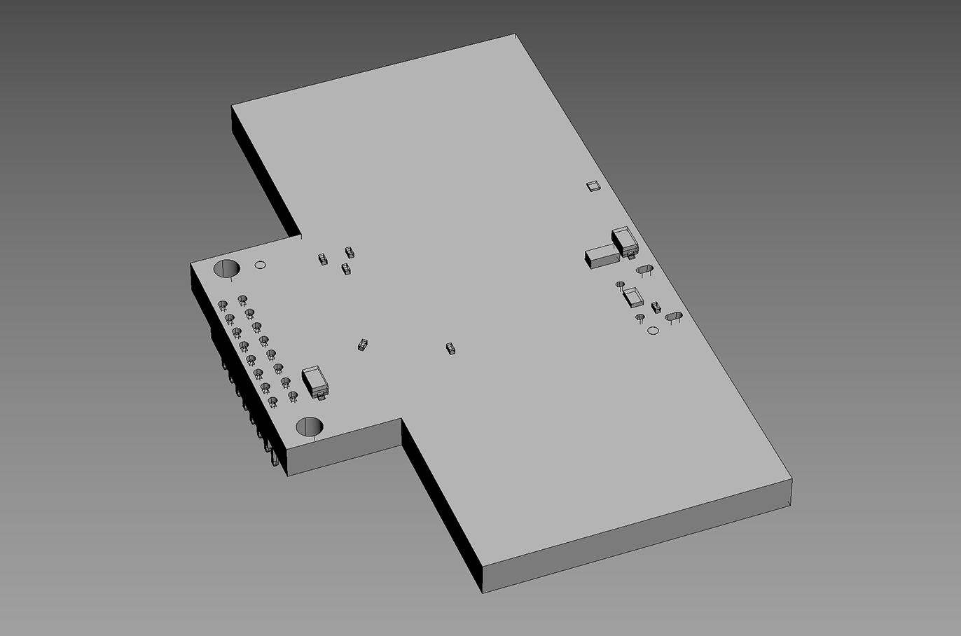
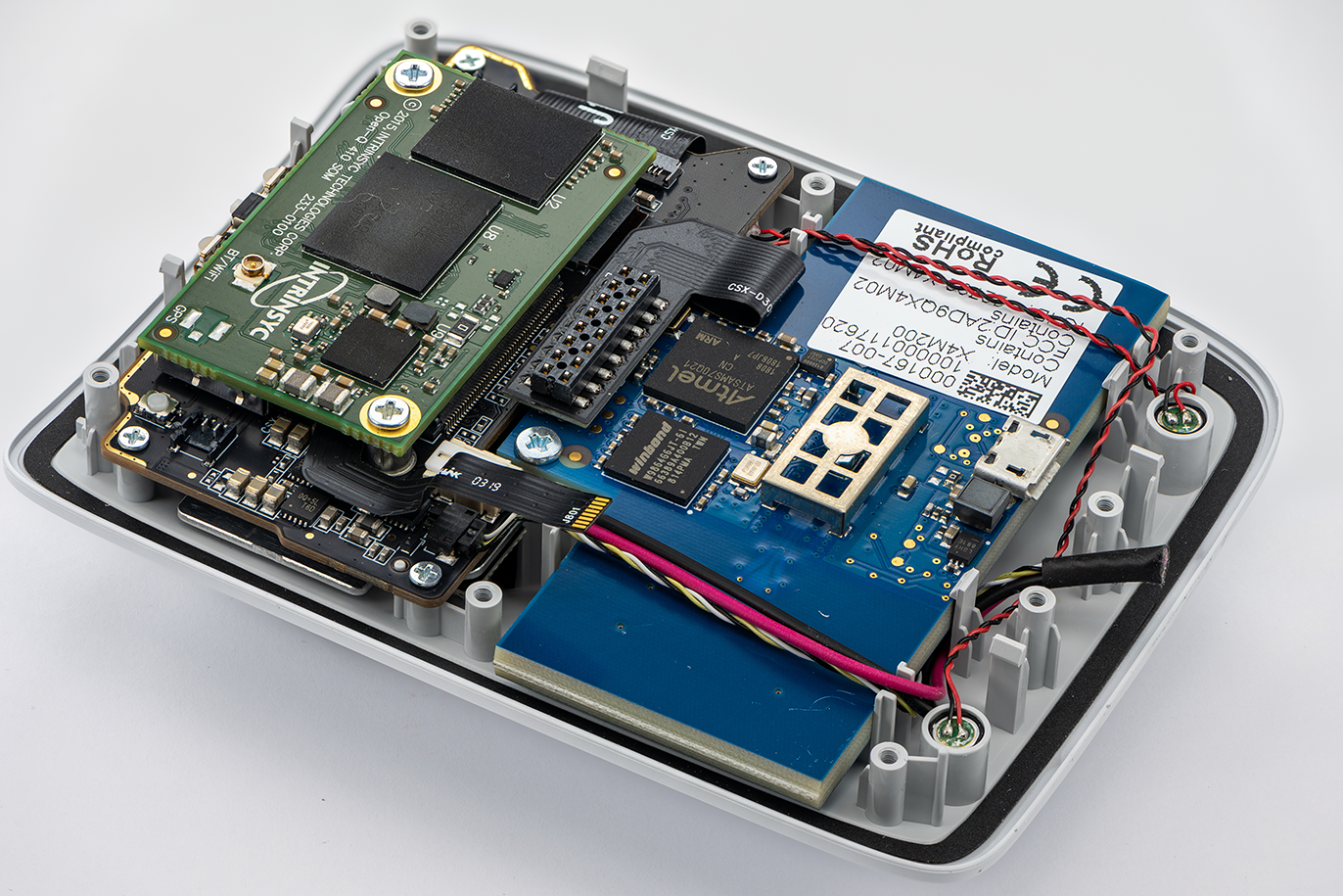
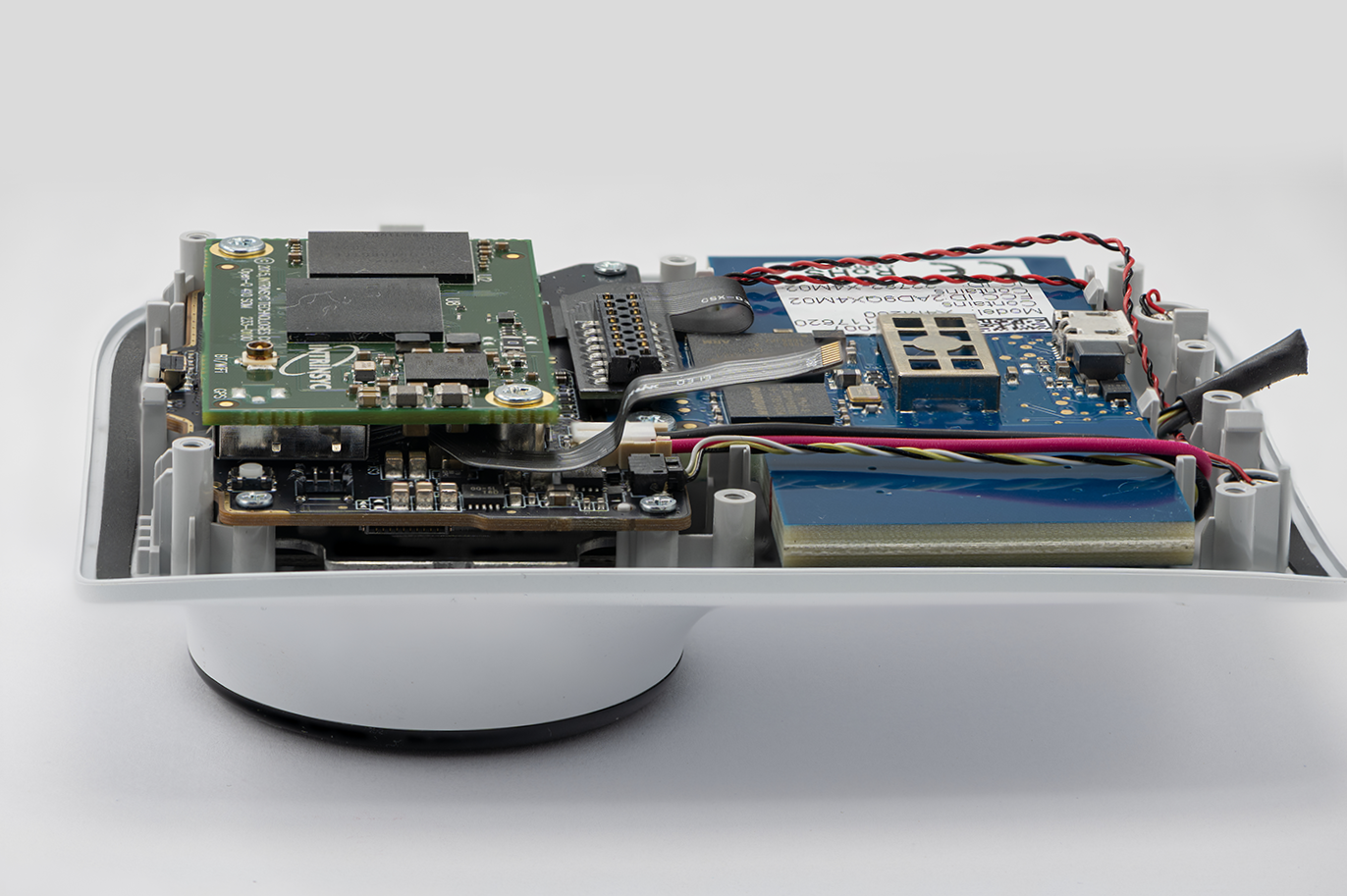
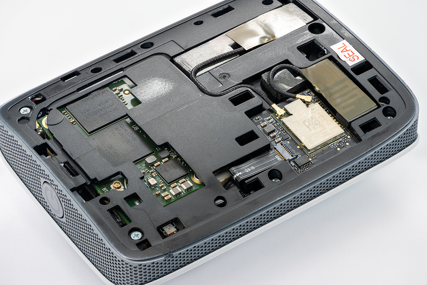
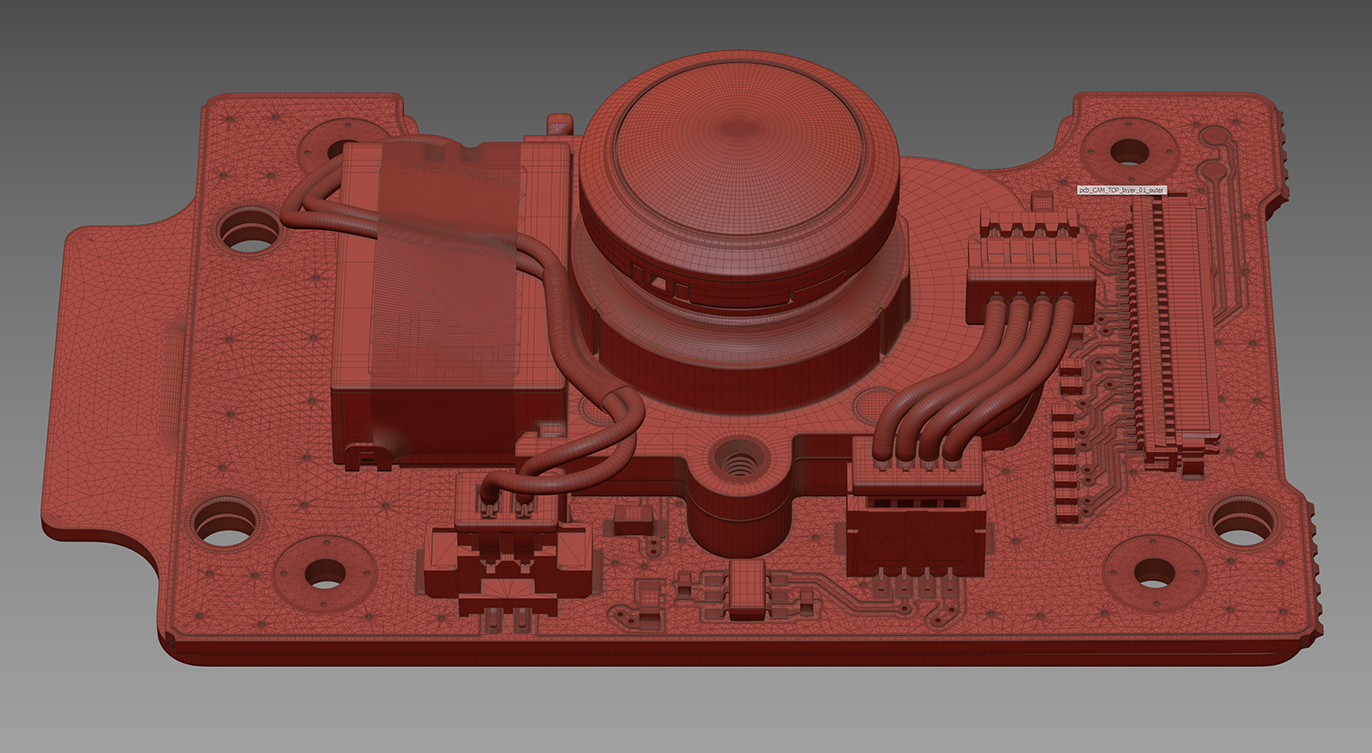
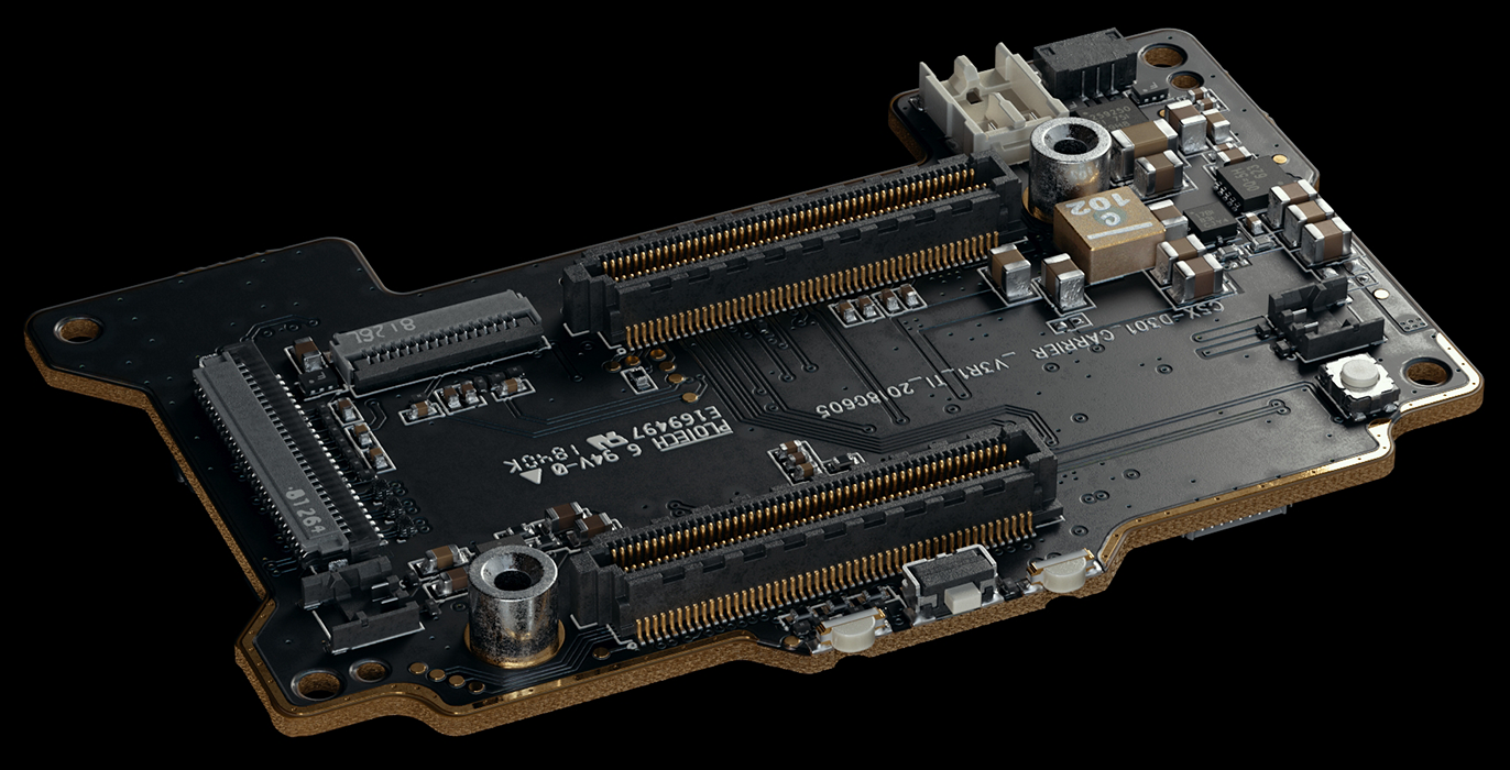
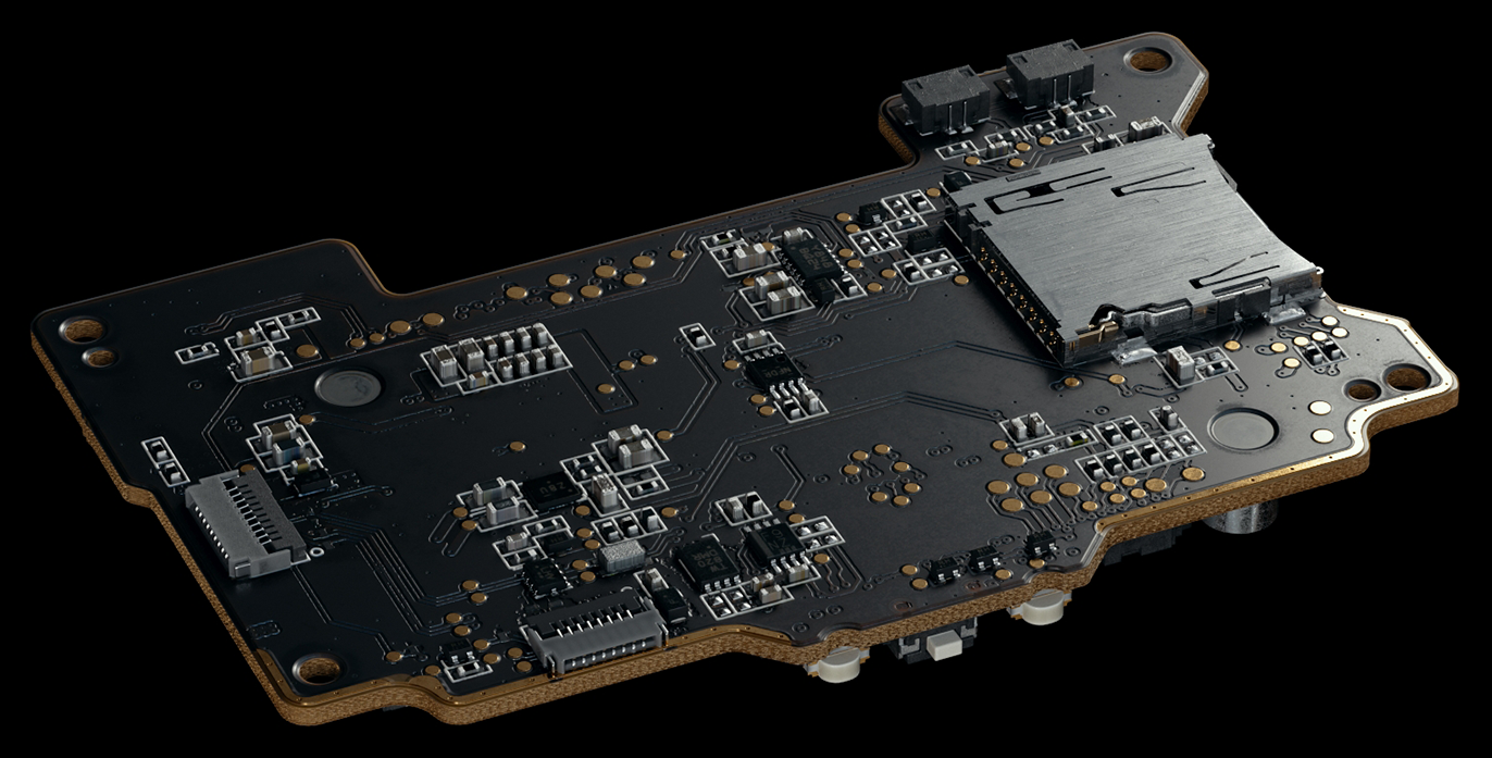
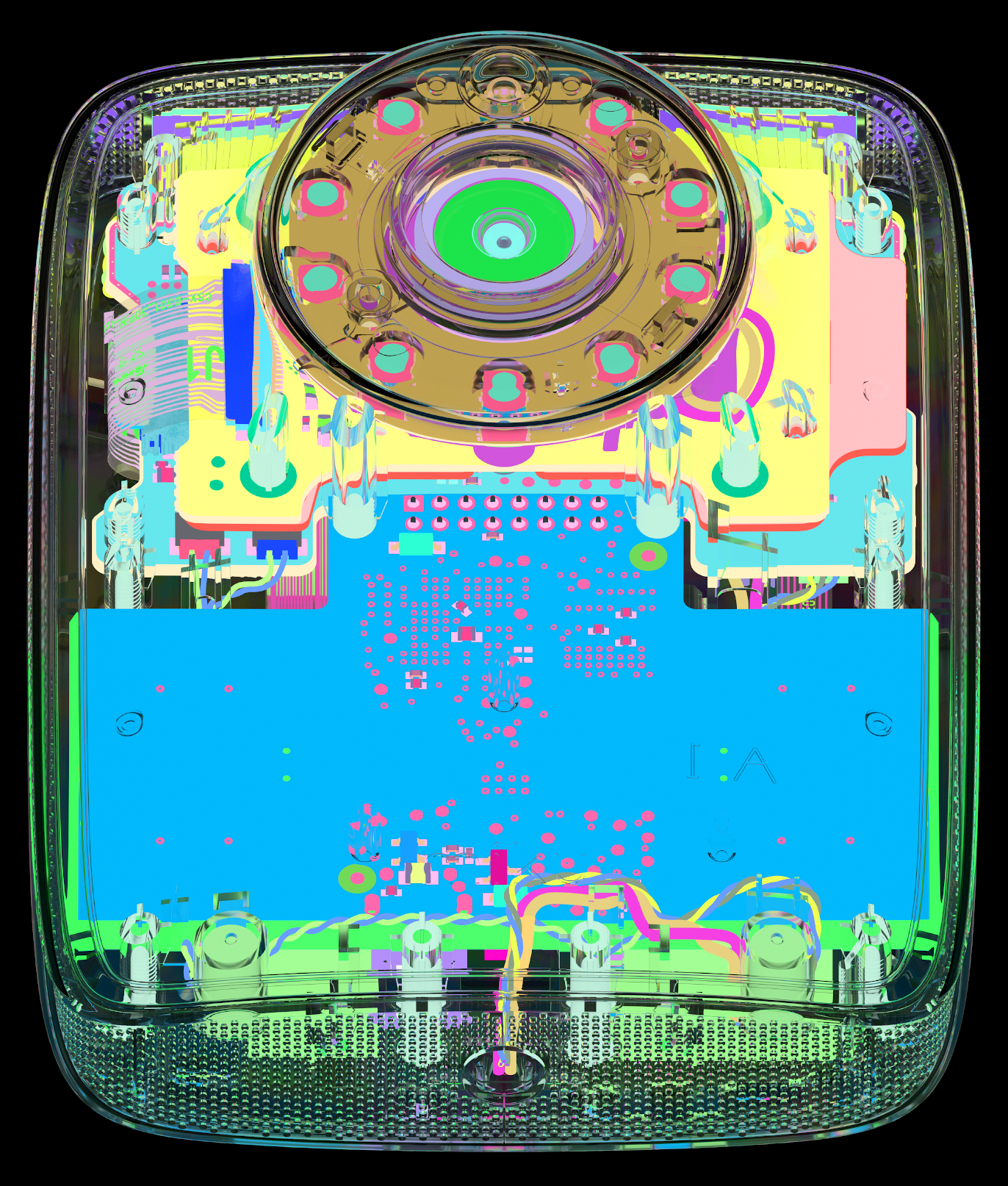
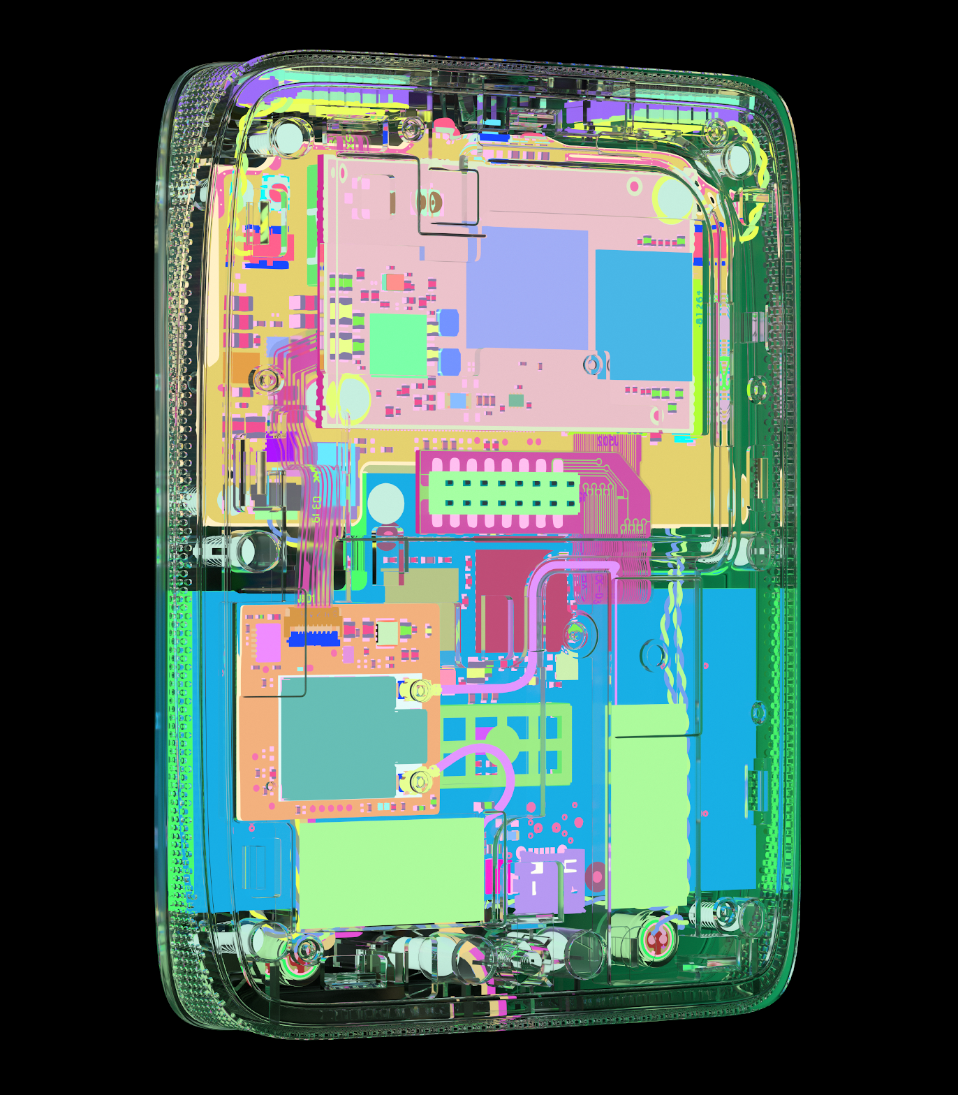
PCBs render
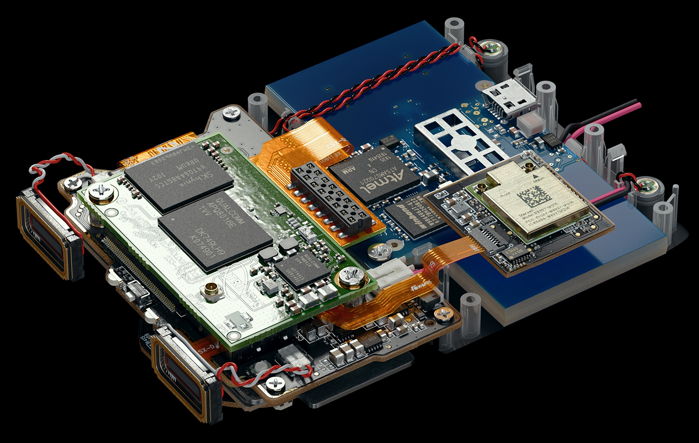
As I mentioned in the beginning, working with the internal parts was the main reason for choosing this baby monitor. The internal structure consists of 6 blocks:
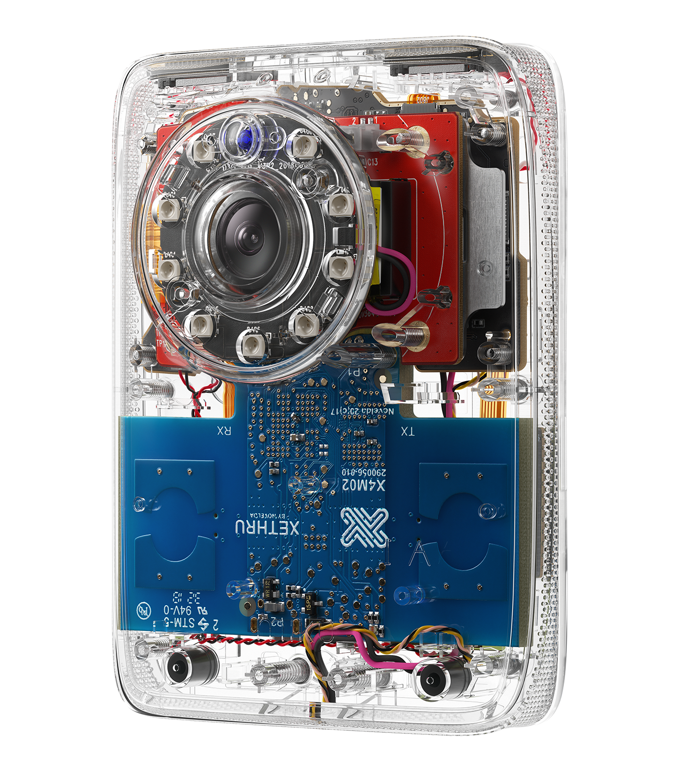
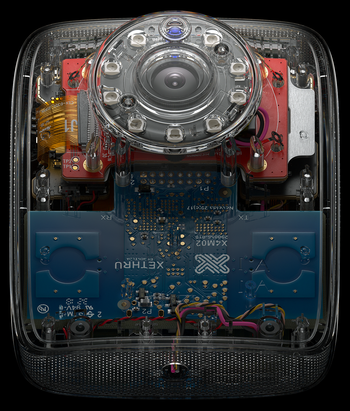
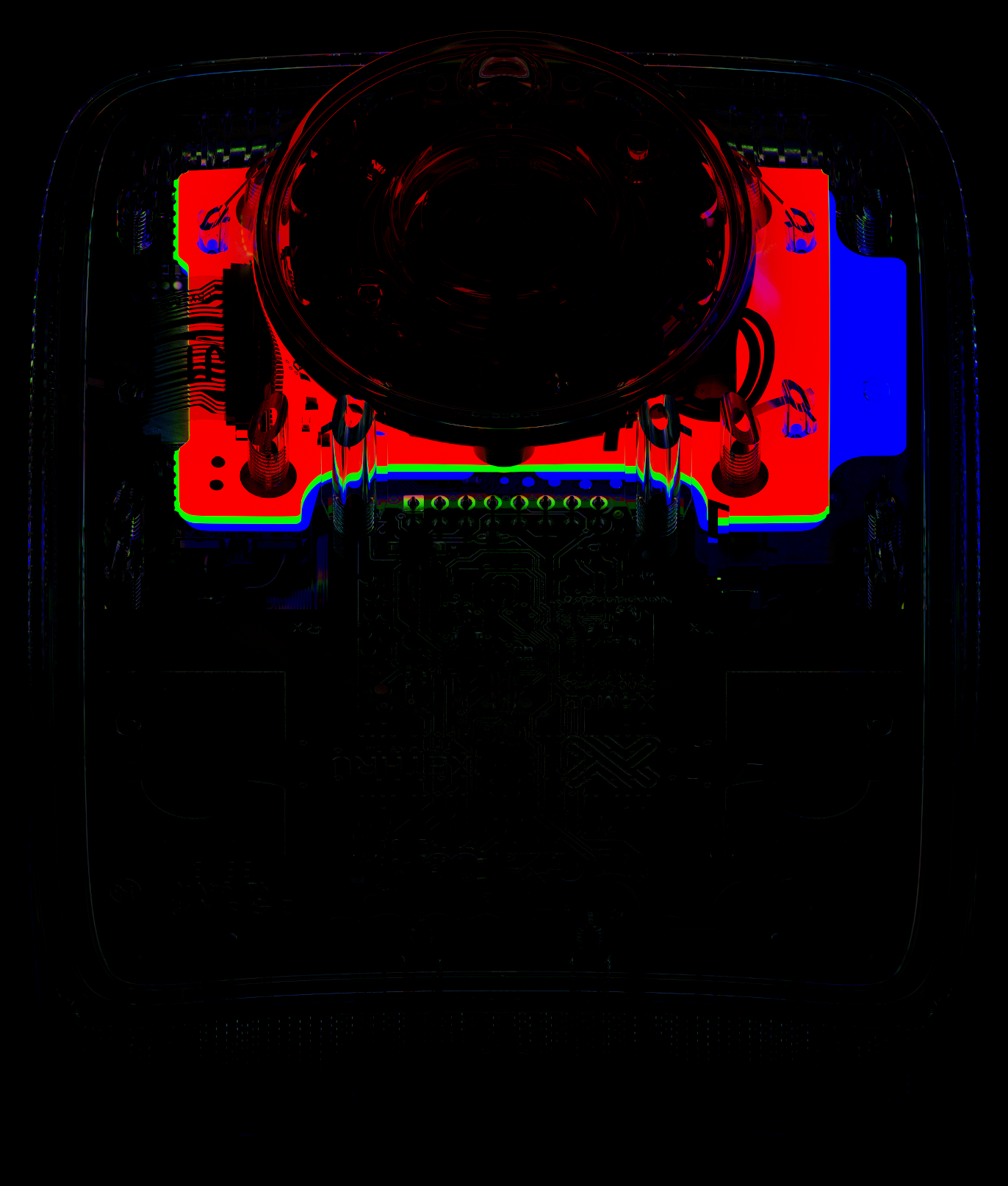
Block of IR emitters and the controller - black, circular
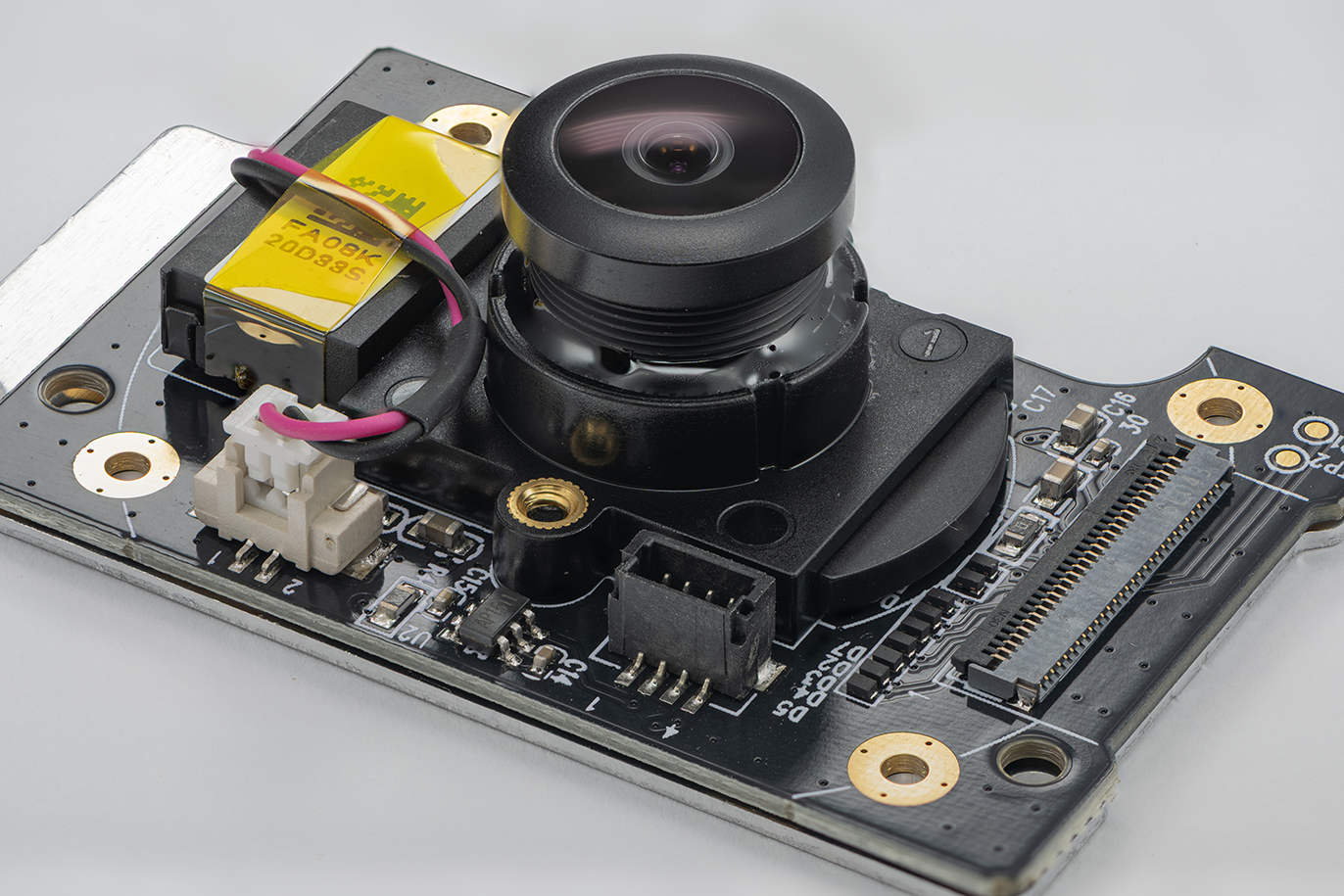
Assembly of the camera module with the controller - red
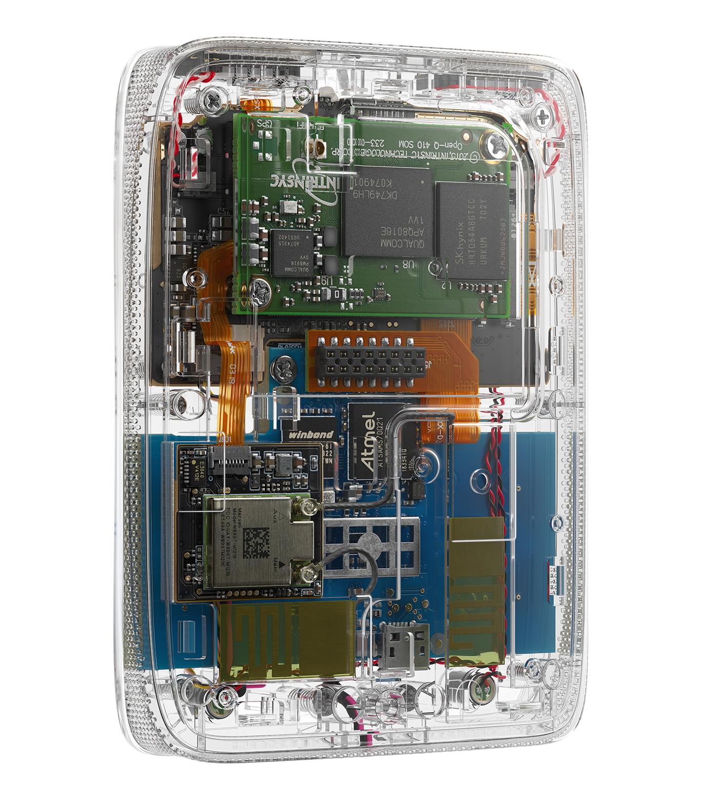
Memory board with SD-Card Controller - black PCB behind the camera assembly
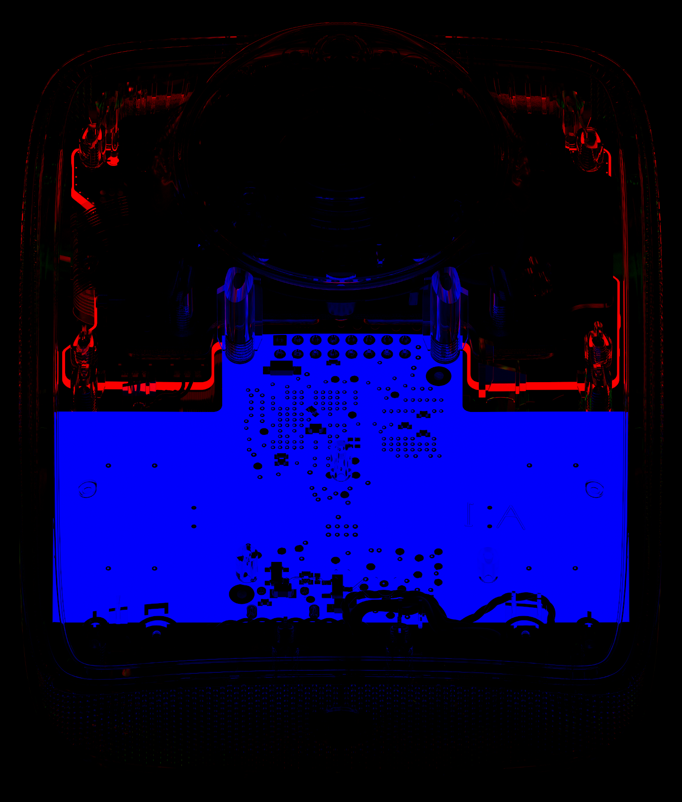
Intrinsyc 410 SoM Board - green
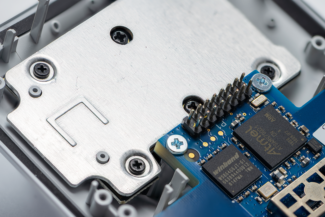
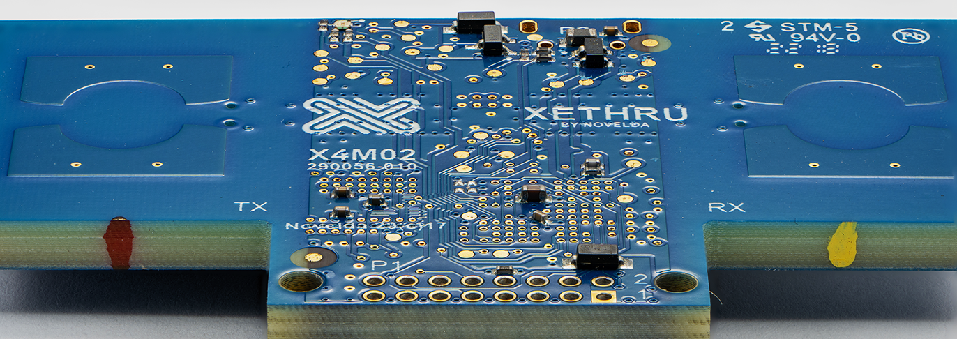
Radar Sensor SoC Board - blue
Marvell Wireless Controller - small black
Assembly of the camera module with the controller - red
Memory board with SD-Card Controller - black PCB behind the camera assembly
Intrinsyc 410 SoM Board - green
Radar Sensor SoC Board - blue
Marvell Wireless Controller - small black
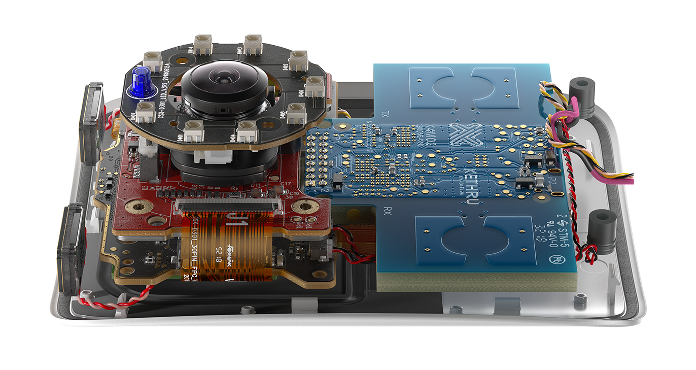
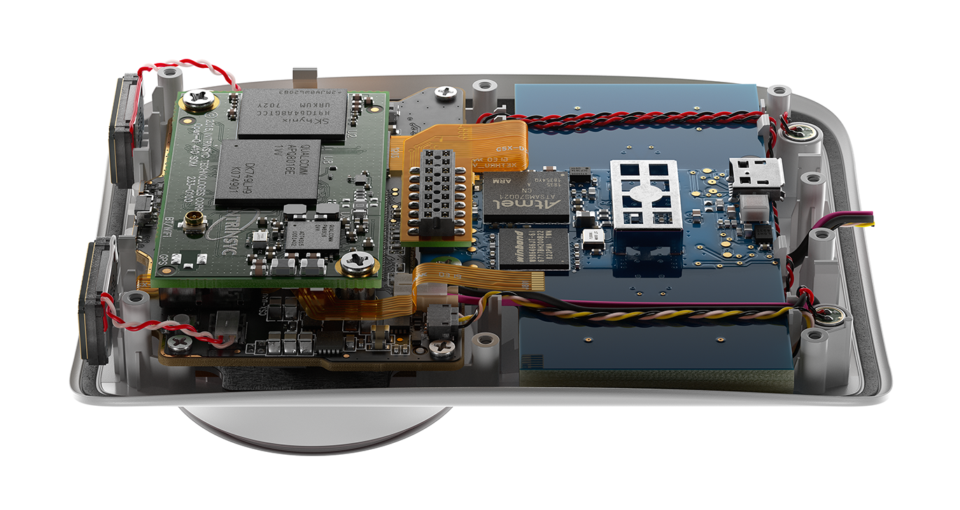
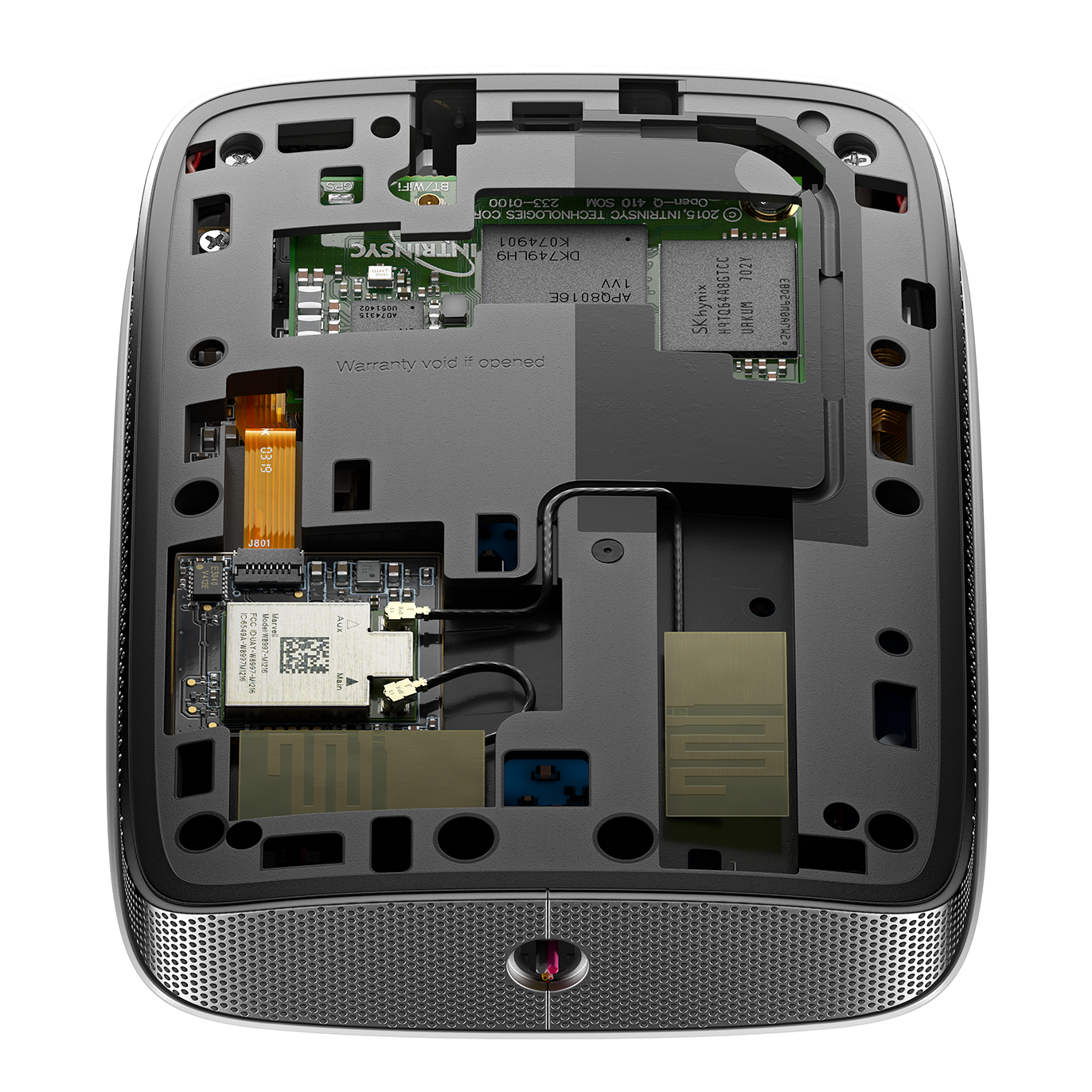
Also, inside the case, there are speakers and directional microphones, wiring, FPC connectors, and flexible wireless antennas.
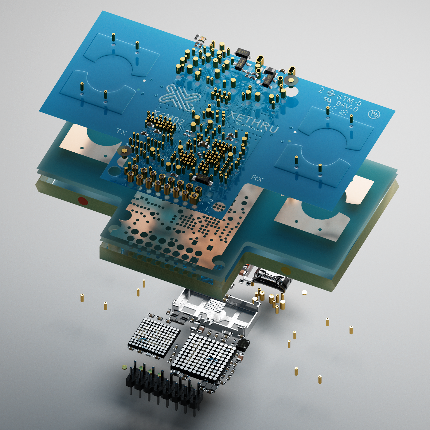
Renders with a transparent body
The most exciting task on the project for me was working on the combination of electronic components, assemblies, and the baby-monitor case itself. During the work on the project, I had been constantly checking the internal case design so that it matched the PCBs mounting.
I believe that same as a product surface design, the engineering has its own aesthetic too. And that was the main goal to me - to show all that beauty assemblies together.
Renders on a black background
During the work process, I realized that I will be very limited in the choice of angles and lighting if I only render "white on white". Therefore, after finishing the central part of the project, I decided to try another exercise - rendering on a dark background, using the "low key" technique.
I found it interesting to try to light each scene with the minimum number of emitters (ideally one).


This method works great with dark backgrounds, creating the dramatic contrast and the ability to "dissolve" the object into the environment by shading it.
Opposite to rendering on a white background, I decided to avoid orthogonal and formal angles, building a composition based on abstract forms, paying more attention to the masses and shape they get in the frame.
As a result, I got a series of noir renders, where you can read more into the texture of some materials and get a feel for the shape of the object.

The Process and Behind the Scenes
As I initially wanted to try working with internal electronics, I started researching how the PCB boards are usually photographed and rendered.
I have noticed that often the style of lighting and working with models and shading seem to demonstrate a lack of understanding of the technological processes of creating PCBs and microelectronics production.
In most cases, I have found that the shading of the PCB was similar to the regular scale objects, which might not be the best choice, in my opinion.
In most cases, I have found that the shading of the PCB was similar to the regular scale objects, which might not be the best choice, in my opinion.
Since I am not an engineer myself and only had some experience with this topic in my youth, I decided to pay attention to references, research, and preliminary preparation.
The original 3D model that I worked with back in 2017 was a CAD outer shell (STP) with dimensional blocks inside, representing the silhouettes of the PCB with simplified shapes for large components. The PCB mounting elements of the case body were also made very sketchy.
It became evident that these parts can be used only as a basis for modeling and detailing next.
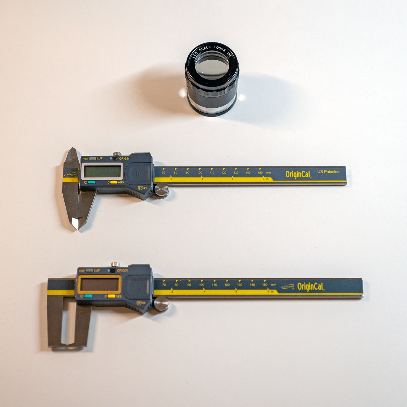
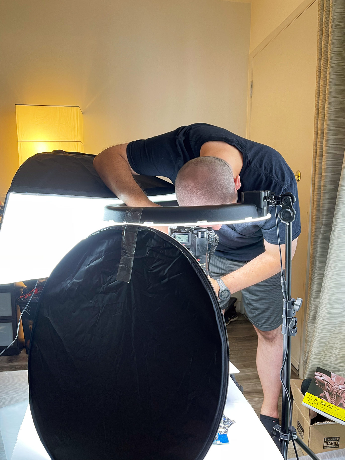
For further work, I needed information about the real PCB assemblies. I ordered three used MIKU kits on e-bay to disassemble and reverse engineer them next. My main reverse engineering tools were a pair of digital calipers (for external and internal measurements), a magnifying glass with a dimensional grid, and macro photography.
I had not yet chosen the exact technique for creating 3D assets at the moment of photo-shooting, and I decided to shoot each board from both sides in the highest possible resolution to make it possible to use the photos not as a reference only but also as a source.
I have used a Nikon z7ii 45mp camera and a Nikkor 105mm f2.8 macro lens for macro-shooting, and I also built a small macro-studio at home.
Since some boards were glossy and reflective, it was essential to get the soft highlights on the surfaces, avoiding the overbright and sharp specular reflections. I have used a 45x45cm lightbox, 5 LED lights, and one ring light.
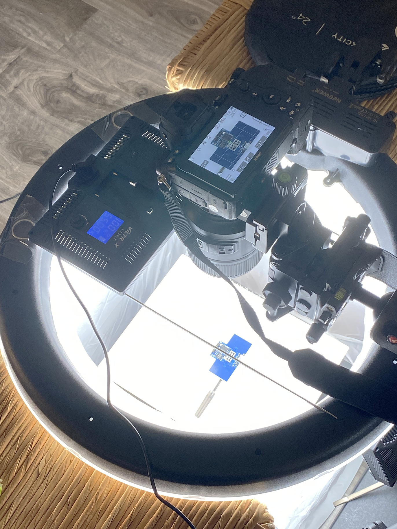
As the thick PCB coating creates the polarizing effect it made sense to use a polarizing filter to control how much light I need in the reflections.
I have used the photo-stacking technique and the focusing rail to get sharp shots with the macro lens, which has a minimal depth of field, even with the closed aperture.
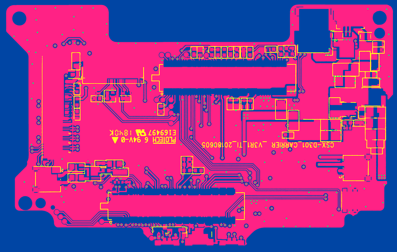
As a result, I made 10-15 shots for each side of the board, moving the camera along the Z-axis using the focusing ramp. Then I loaded these takes into the Helicon Focus software, which merged these takes into one sharp orthogonal picture of the PCB.
The final resolution of the obtained textures was around 15000pix wide, which allows using them for anything - vector tracing, creating masks, and shader layers.
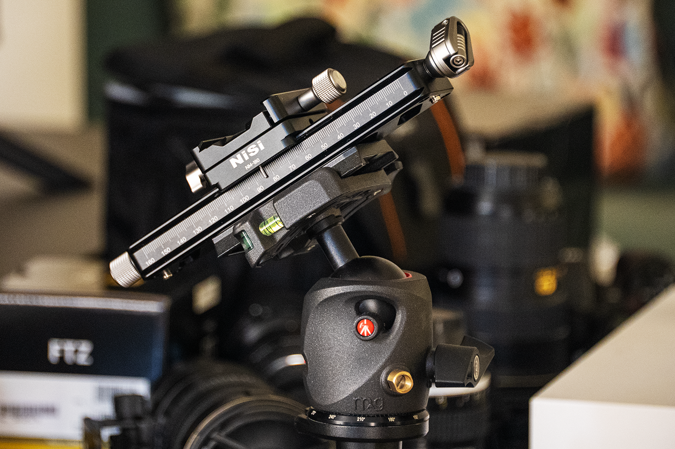
Camera Focusing Rail for macro photo-shooting
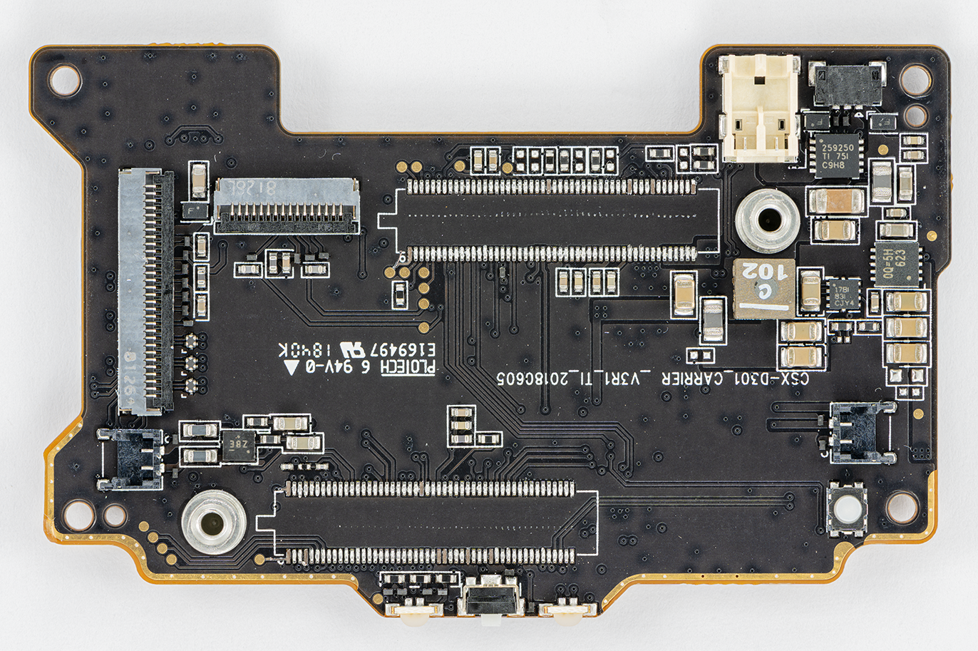
Memory Controlling PCB Source Photo
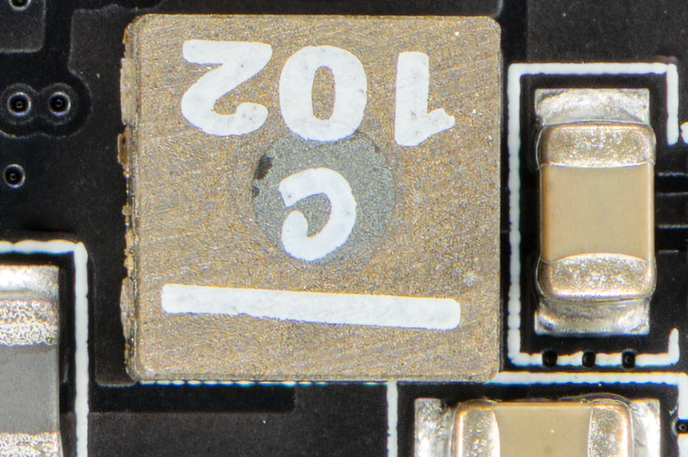
Memory Controlling PCB Source Photo 100% crop
Some of the reference photos of the MIKU baby monitor
During the research, I realized that a photo-realistic result is impossible without SSS because, at this scale, all tiny and thin-walled objects begin to transmit a lot of light, which creates very soft and filling colored lighting inside the circuit board assembly.
This aspect has become key in favor of choosing a render engine for the project.
This aspect has become key in favor of choosing a render engine for the project.
The FStorm renderer is a photo-realism-oriented engine regarding the physics of light and shading. The most important was the quality and speed of the SSS engine in FStorm render

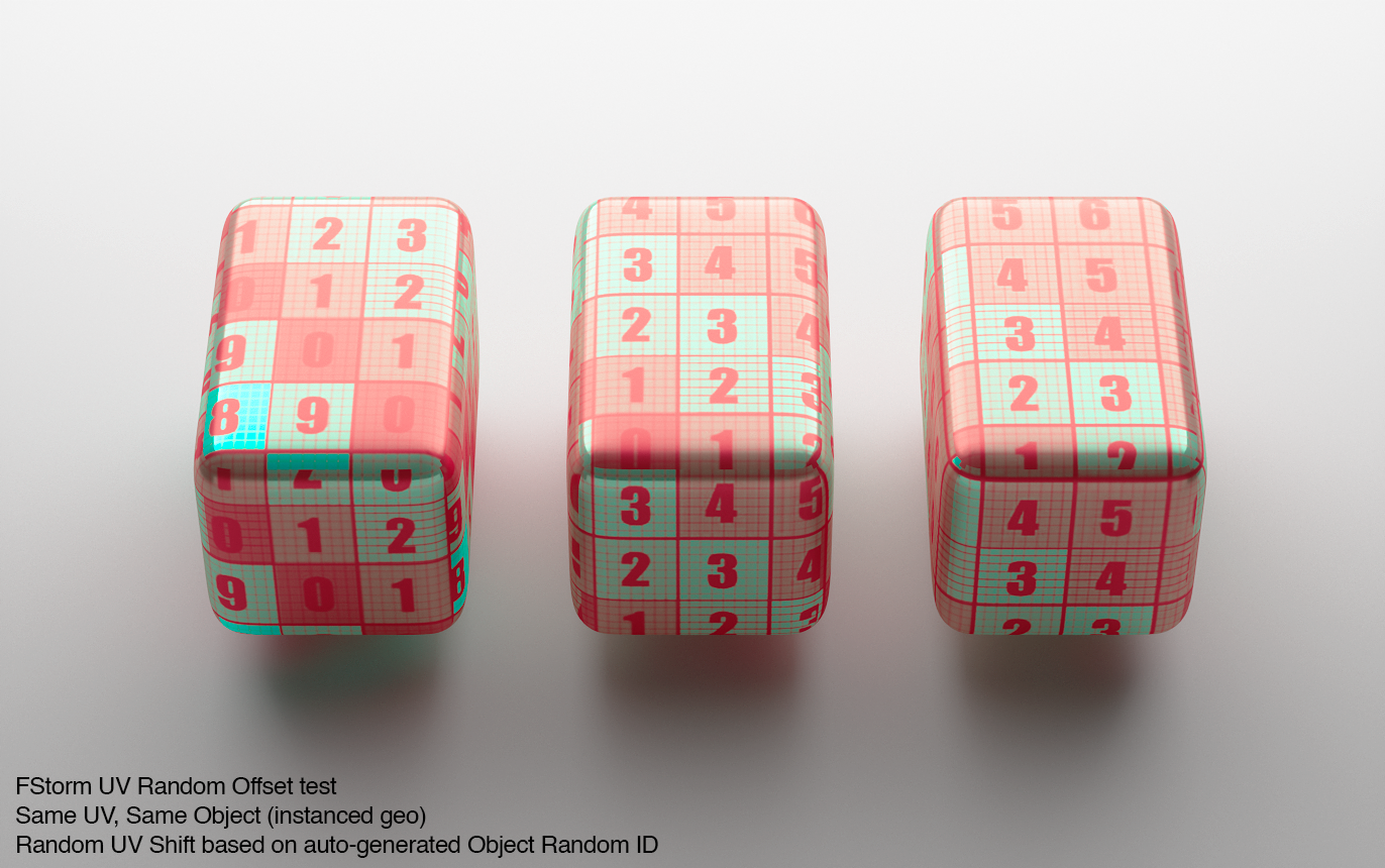
In addition, FStorm can offset the UV of an object based on its random ID, which is generated automatically for each object in the scene. This UV trick allows me to use the instanced geometry for components geo, and a single shader while varying the texture's color and getting different bump mapping in the close staying parts, such as capacitors or resistors.
In the process of working on the PCB, I used different techniques. To create the camera controller board, I traced all the paths in Illustrator and used this vector for further modeling. It made sense because the paths on this board were deep enough, and there were not too many of them. Also, this PCB assembly had paths on only one side because it is covered with a metal screen on the other. The tracks on this board have been modeled as real geometry.
Camera Assembly viewport geo
Camera Assembly test renders
Memory controller PCB test renders
Working on the layered masks for the Memory Controller PCB
Working on the PCB assembly.
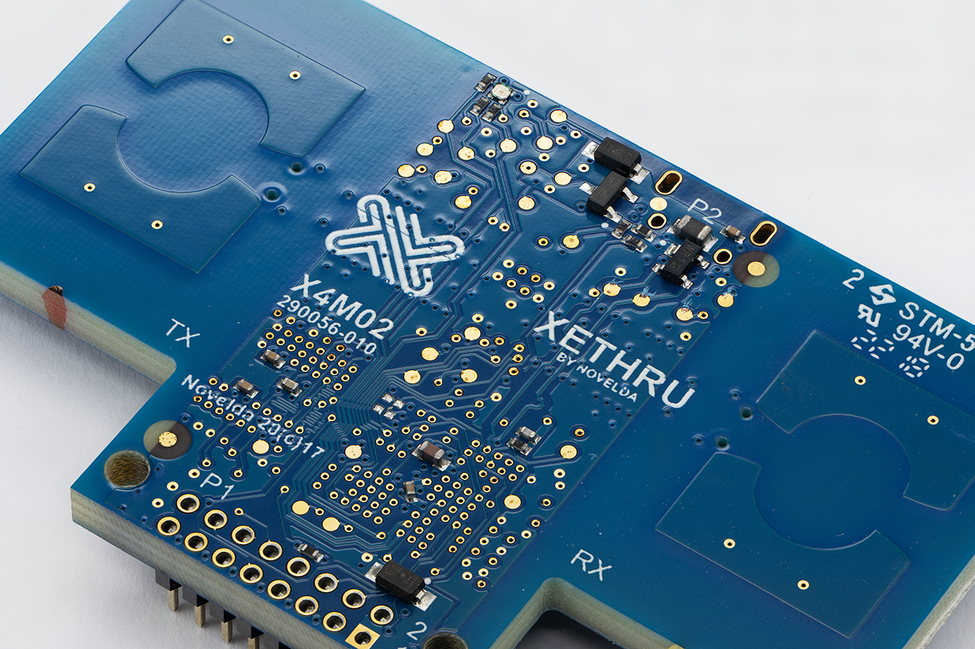
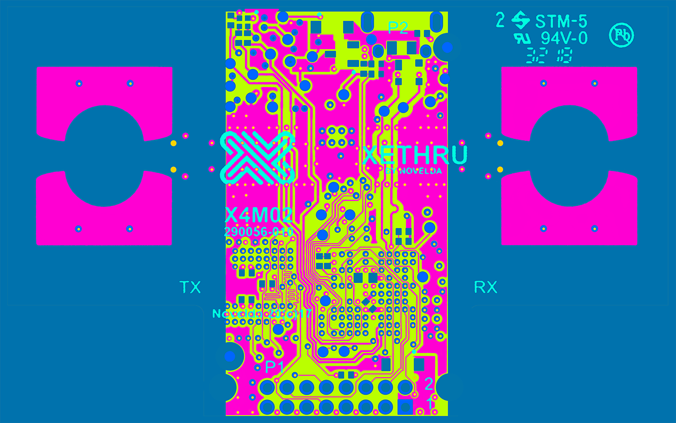
However, the most exciting part for me was the work on the big blue PCB - the sensor controller “Radar Sensor SoC Board”.
It is a large, double-sided, multilayered PCB assembly with many paths and an interesting complex layout. In addition, due to the fact that it is quite large in thickness (4mm) and the fact that the top layer of varnish is semi-transparent, the board lets in a lot of light, painting it in deep blue.
Due to a large amount of light inside the fiberglass layers, you may notice a few more layers of copper plates, which cast shadows inside the material.
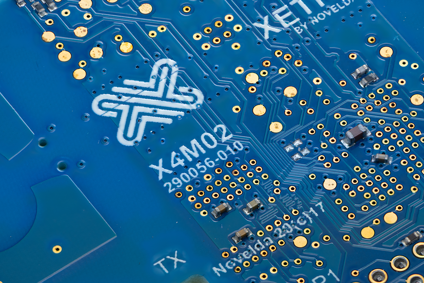
Radar Sensor SoC Board reference photo closeup
It was a real challenge that required an in-depth study in all aspects. In addition, the top layer of coating was so thick that it created the effect of "glazing" the paths on the board's surface.
From the beginning, it became clear that it would be challenging and time-consuming to achieve such a look using real-geo modeling, which prompted me to choose a technique based on textures.
It was also not evident whether it would be possible to achieve this effect using procedural methods or I would have to use 3D sculpting methods to get the proper displacement height maps.
Radar Sensor SoC Board reference photo
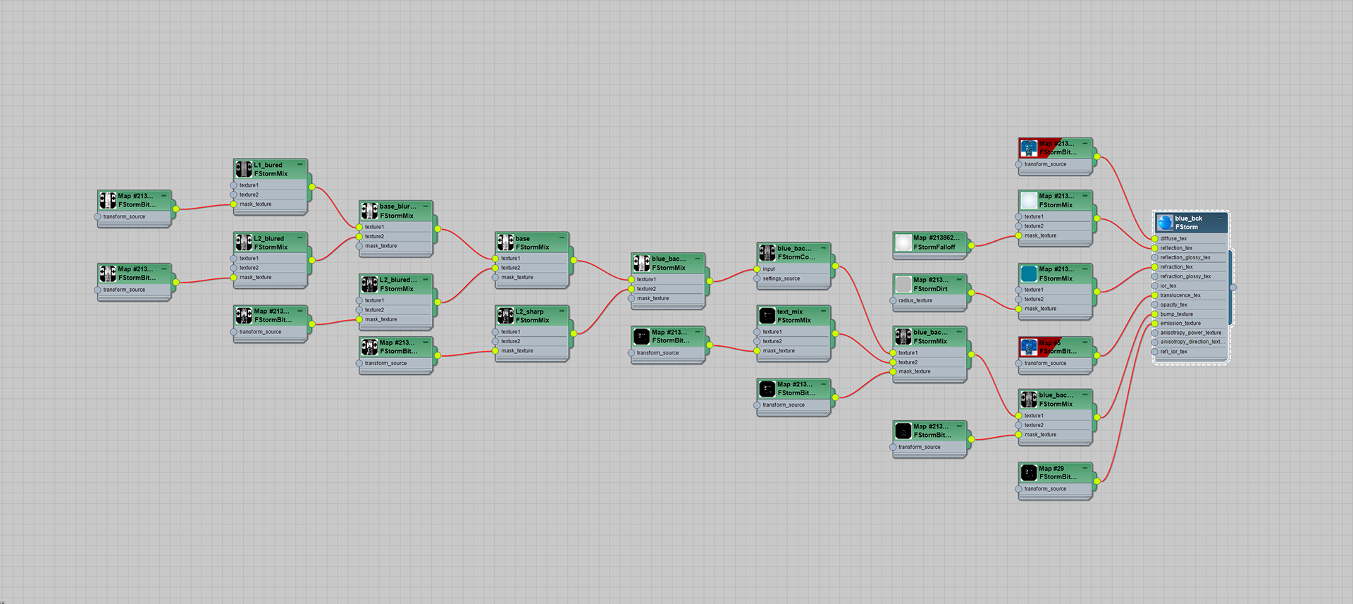
Finally, I achieved a good result using a combination of the parallax bump method (a technique that allows you to achieve a quality comparable to the micro-displacement at the normal-mapping speed) and multilayered bump texture generation using a mix map.
The final height map has seven layers mixed by masks with different amounts of blur. To increase the rendering speed, I used blurring of individual masks in Photoshop because procedural blur during the calculating before rendering takes a lot of time due to the high resolution of the textures.
Working on the layered masks for the Radar Sensor SoC PCB
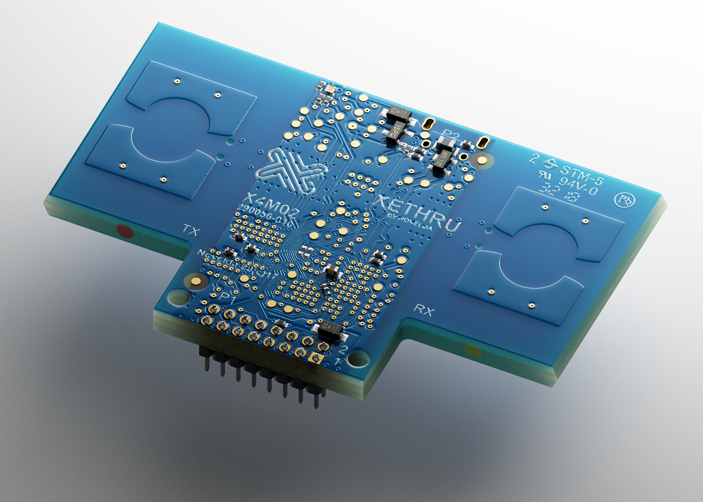
I also added some geo layers to the inside of the board to create a sense of inner shadow and uneven light penetration. The golden contact plate geo has a procedural blend with the PCB surface, enhancing the glazing effect.
I deliberately avoided using any kind of imperfections such as dust, dirt, wear marks, or grease marks.
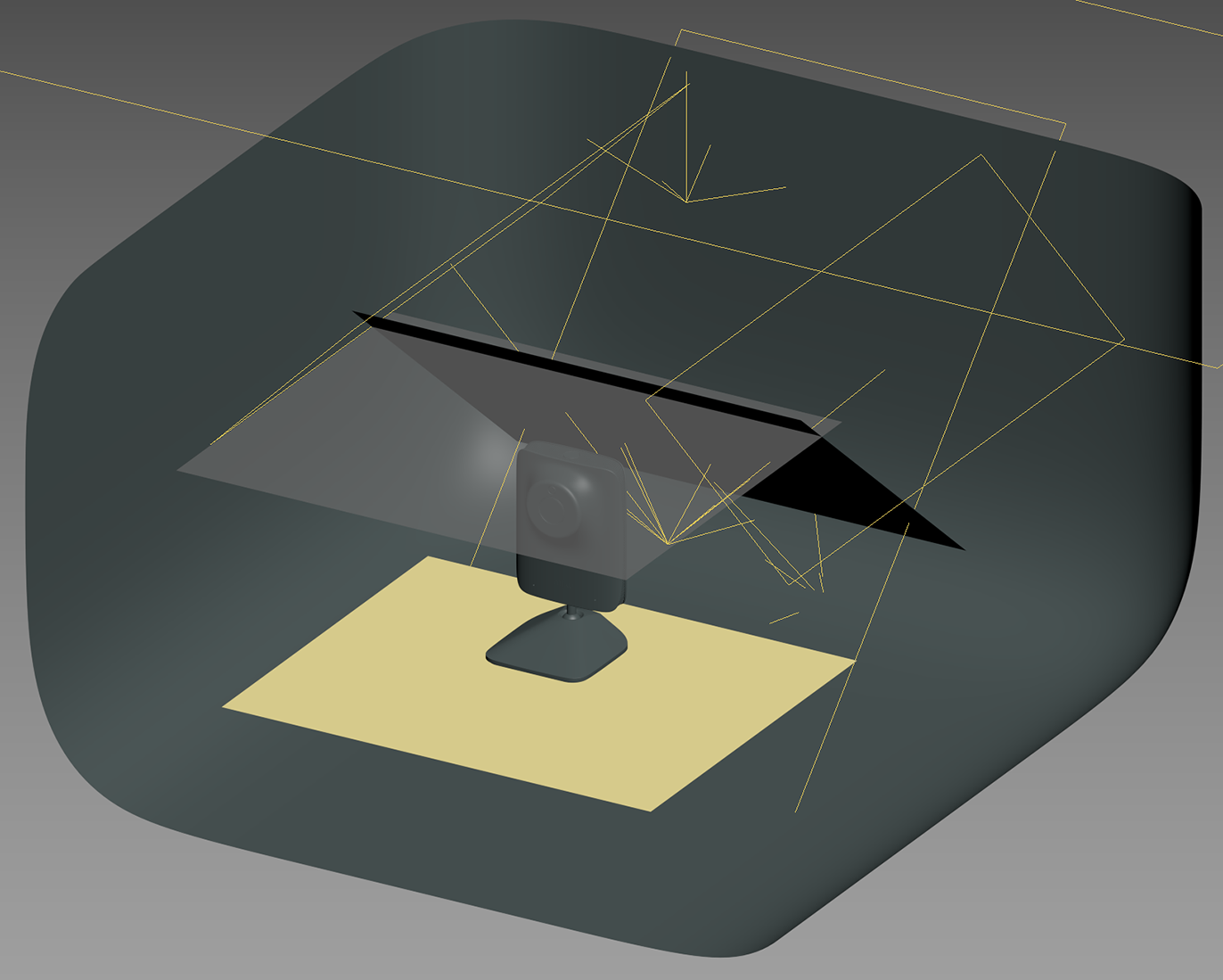
Lighting
From a technical side, all the lighting was done with separate lights, using procedural gradients. In some cases, I used self-luminous plates with gradients without generating a diffuse channel, which created only a specular reflection on the surface.
It is interesting that in FSorm you cannot use light sources with the invisibility mode (otherwise, they will not generate the Specular channel), so I had to use methods close to real studio photography when the light source can only be outside the frame.
Render and final postwork
Using real-time GPU rendering allowed me to keep post-processing work to a minimum. Mainly I worked with contrast.
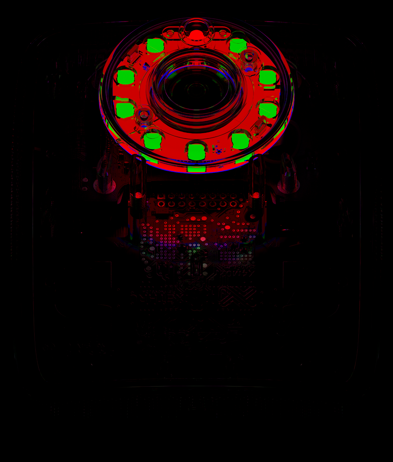
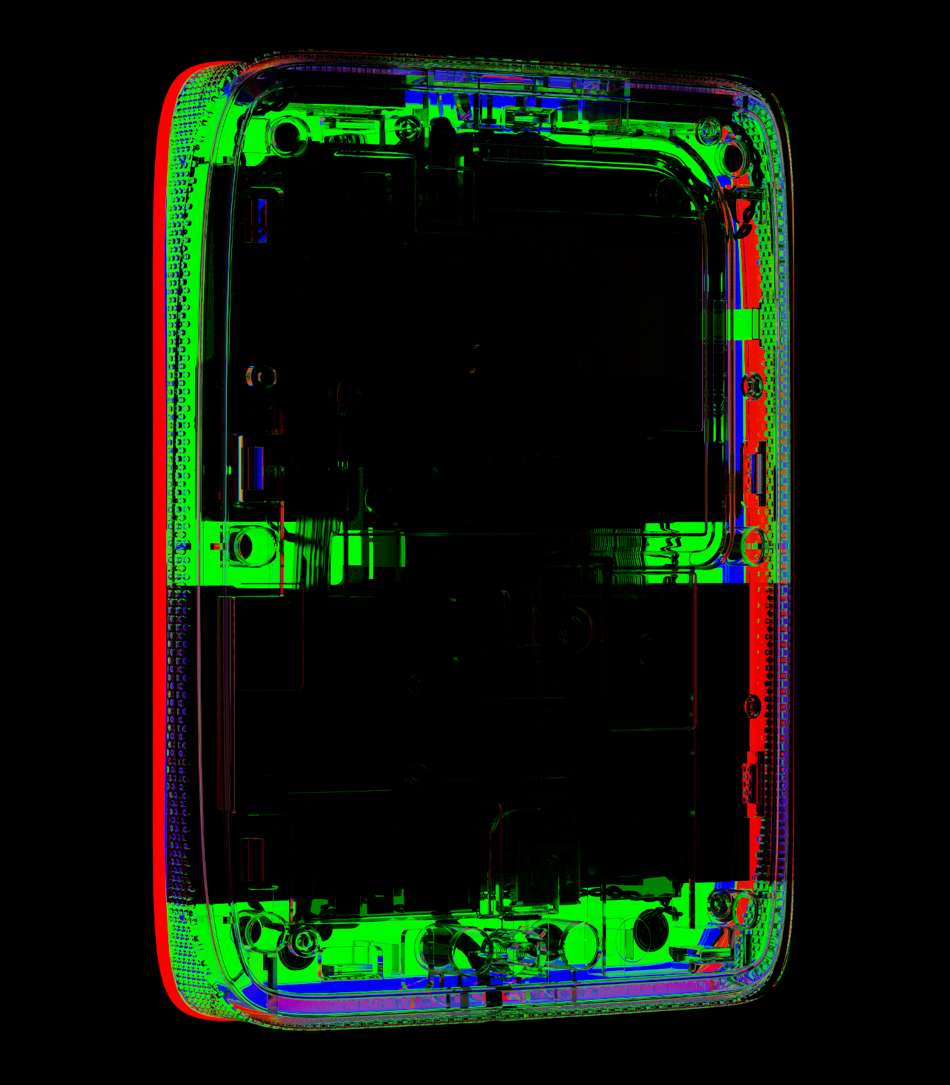
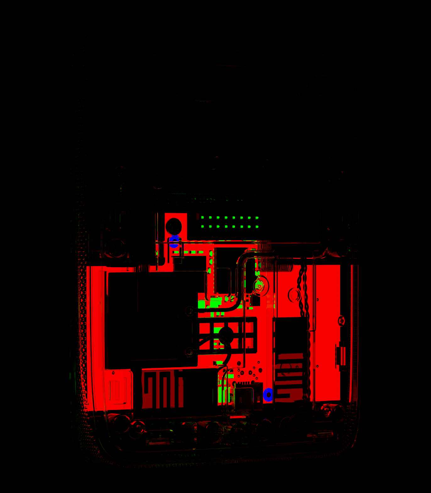
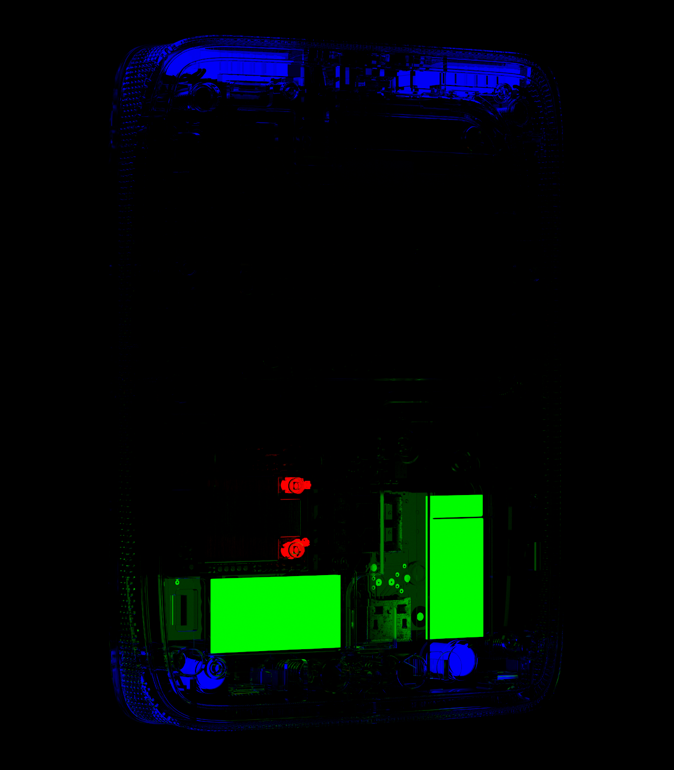
To be able to adjust individual elements, I used RGB masks, some of which themselves look like art objects.
Each frame rendered at 4k wide resolution on a 2x RTX 3090 PC. The average render time for a frame was 15 - 35 minutes. In some cases, such as rendering with a transparent case body, the time increased to 1 hour per frame.
Thank You